
![]()
![]() Narrow down by specifying conditions
Narrow down by specifying conditions
現在1888件がヒットしています。check

table of contents
1.What is a high-voltage gate driver?
2.What kind of product? What kind of protection does it have?
3. the NCV57000 series! !Make full use of
4. What are the points to be noted in the layout when using the magnetic system Galvanic isolated type?
1. What is a high-voltage gate driver?
A high-voltage gate driver has a large 2 The group is divided into product groups.
・ Junction isolation type
・ Galvanic isolated type
Here's a quick overview of what each type is.
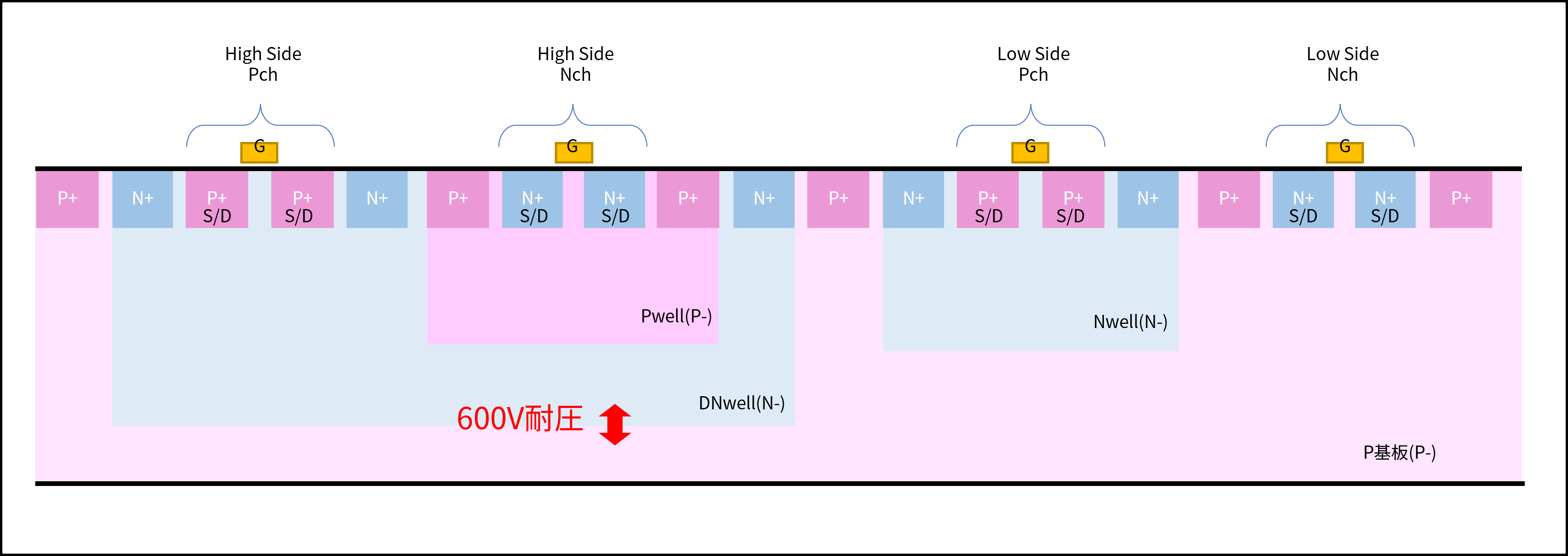
What is Junction Isolated type?
"P-type semiconductor" and "N-type semiconductor", so-called PN Junction 's reverse withstand voltage, are used to ensure withstand voltage corresponding to high voltage. It is a gate driver that has such a configuration. Figure 1 shows an image of the cross-sectional structure.
As you can see, P and N are physically connected, so in other words, "there is a direct conductive path," and it is generally called a "non-insulated type." I feel like
What is Galvanic Isolated type?
In contrast to the junction isolated type, it is a gate driver that is physically isolated, in other words “no direct conduction path exists”.
There are three major methods of insulation as follows.
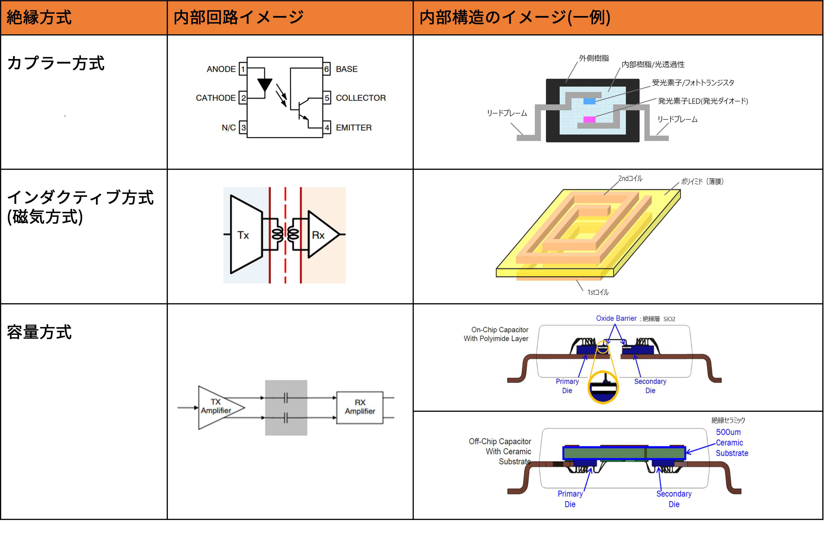
ONSEMI's Galvanic Isolated type insulated gate driver has coupler type and inductive type products. We are releasing new products one after another, and are expanding our lineup so that we can consider the optimal gate driver as a set with power semiconductors.
For this content, please also refer to the digital isolator article from the link below.
What's the difference from other companies! ? What are the features of Onsemi's digital isolator?
In the next chapter, we will introduce our flagship products, NCD(V)57000/NCD(V)57001.
2. What kind of product? What kind of protection does it have?
About product
The NCD(V) 57000 series was released for the first time in 2019 as a Flag Ship model of galvanic isolated gate driver products. In addition to the main function of driving IGBTs and SiCMOS, various protection functions are installed.
Since then, we have expanded our lineup by developing products with functions optimized for various applications and products with selected functions. With such a large lineup, it can be difficult to decide which one to use, but I believe that this reflects Onsemi's development philosophy of enabling customers to select the optimum parts for their various uses. If you have trouble choosing, please contact us anytime.
Now, let's introduce the characteristics and function matrix table of the NCD(V)57000 series. The NCD(V)57000 is a 1ch type (single product), but the lineup also includes 2ch output products with a bridge configuration. There is a link to the manufacturer's HP at the bottom of this article, so please check there.
The upper part of the product name is a consumer product, and the lower part is an automotive product.
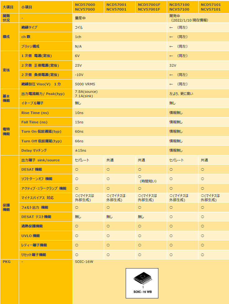
About the protection function
It can be said that the NCD(V)57000 series incorporates most of the commonly required protection functions.
Briefly explained in the table below
|
Table 2: List of protection functions
3. Make full use of the NCV57000 series! !
Below are some points to note when using the NCD(V)57000 series.
For the contents of this item, please refer to ONSEMI's application note. (AND9949-D.PDF) is referring to
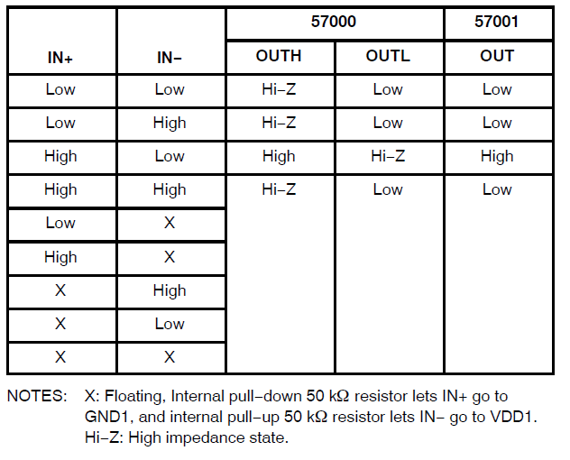
·input (IN+,IN-) and output (OUTH,OUTL) logical relationship
・ 1 Next side input power supply
・ 2 Next side input power supply
・Regarding loss and heat
Details are provided below.
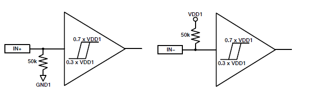
Logical relationship between inputs (IN+, IN-) and outputs (OUTH, OUTL)
Table 3 and Figures 3, 4, and 5 below are excerpts from ONSEMI's application note (AND9949-D.PDF).
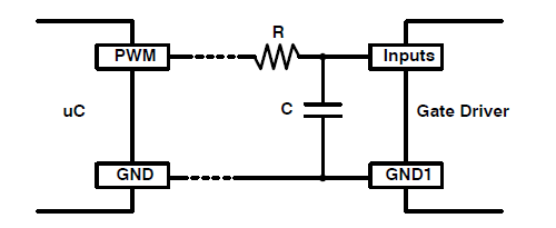
In general, inputs (IN+, IN-) receive signals from a microcomputer, but RC filter circuits can be inserted to improve signal quality.
The values of R and C depend on system requirements such as drive frequency and duty. Also, for the input signal (microcontroller output), a standard CMOS or push-pull drive circuit is recommended, and an open-drain configuration should be avoided.
In the PBC layout, R and C should be as close to the gate driver side as possible to keep the traces short.
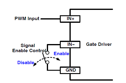
It is also possible to use only the IN+ as the drive terminal and the IN-terminal as the EN signal terminal.
Of course, it is also possible to use only IN-for driving. However, in the latter, the input/output logic is reversed.
Primary side input power
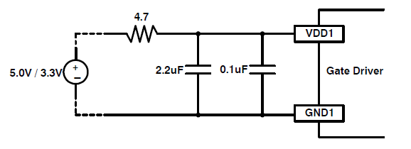
A series resistor and decoupling capacitor should be placed between VDD1 and GND1.
The capacitor should be placed as close as possible to the gate driver IC to filter out high frequency noise and maintain the input bias voltage.
In general, we recommend low ESL and low ESR chip capacitors (MLCC: multilayer ceramic chip capacitors).
Secondary side input power
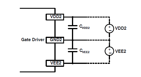
Since the output pin has a high current capability, a very high peak current is generated when the output MOS inside the IC turns on. Therefore, the PCB layout needs to be very careful.
Decoupling capacitors should be placed between VDD2-GND2 and between VEE2-GND2. These capacitors should be placed as close to the gate driver as possible to prevent overshoot and undershoot voltages due to parasitic inductances including PCB traces.
Also, the excessive peak current is mainly caused by the external load capacitance, so it depends on the output MOS gate resistance (external resistance).
For typical applications, 10uF capacitors are required for each positive (VDD2) and negative (VEE2) bias if the gate resistance is greater than 10Ω.
A 20uF capacitor is recommended if the gate resistance is less than 10Ω.
In general, we recommend low ESL and low ESR chip capacitors (MLCC: multilayer ceramic chip capacitors).
Regarding losses and heat
As is common, losses are converted to heat and self-heat. Therefore, the self-heating component is ΔT, and it is necessary to consider ΔT so that the silicon (junction) temperature inside the IC does not exceed Tj_max.
Tj is expressed by the following relational expression depending on the ambient temperature Ta and ΔT.
Now let's think about ΔT. ΔT is determined by the loss Pall and the PKG thermal resistance θja.
Although this is a slightly sidetracked discussion, here we will consider thermal resistance as θ ja. In addition to θ ja, there are other thermal resistances such as θ jc and ψ jt, and we recognize that there are many cases where people wonder which thermal resistance is closest to actual use. Also, when looking at each product of each company, it is mixed, some are all described, and only one is described.
In this document, explanations of various thermal resistances are omitted because they are off topic, but the definitions of each are different, so it is necessary for designers to have a correct understanding of these types of thermal resistances. think.
This is because it leads to various problems, such as selecting expensive components with excessive margins, or underestimating and designing with less margins, and encountering thermal problems. If you are unsure, we recommend that you contact the manufacturer's technology or each distributor's technology each time.
Now back to the main topic.
Now consider Pall 's losses. It can be considered as the total of three major loss elements.
・Input bias circuit loss: PD-IN
PD-IN =VDD1×IDD1
・Loss in the output bias circuit: PD-OUT1
The operating power of the internal logic circuit, measured under no-load conditions. Equivalently, it can be considered as the switching loss of the internal circuit.
PD-OUT1 = (VDD2 x IDD2) no-load + (VEE2 x IEE2) no-load
・Loss in the output drive circuit: PD-OUT2
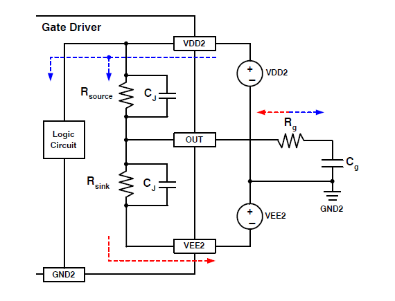
It consists of the total loss due to the on-resistance of the output stage MOSFET of the driver IC and the gate resistance of the external power device.
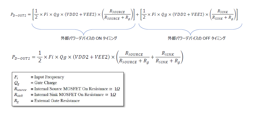
For reference, see Figure 8 below for an image of the power path between the output stage of the driver IC and the external power device.
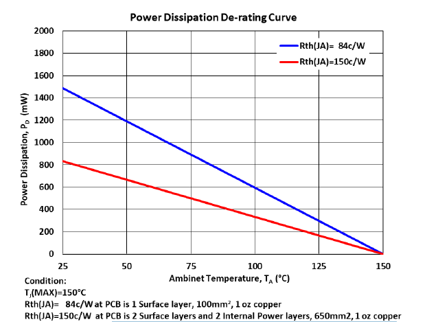
Summarizing the loss and heat, the maximum allowable power dissipation (PD) at the ambient temperature (TA) can be calculated using the following formula when the maximum junction temperature Tj_max is 150°C.
Figure 9 shows the power derating curve for the NCV57000 series based on a specific PCB layout, layer and surface area.
Other points for use
Points to consider, such as how to determine the constants of peripheral components (calculation formulas) that could not be described in this article, are described in ONSEMI's application note, so please check it from the link below.
ONSEMI Application Note: AND9949-D.PDF
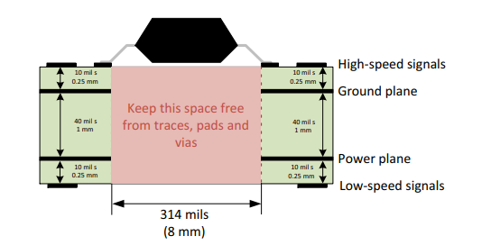
4. What points should I pay attention to when using the magnetic Galvanic isolated type layout?
When using a magnetic galvanic isolated type gate driver, it is important to secure the magnetic path in order to properly transmit the primary side signal to the secondary side. Therefore, please refer to Figure 10 together with the following precautions for board layout.
・On a multilayer board, do not place GND patterns, signal patterns, vias, etc. directly under the gate driver.
・Do not place other ICs on the back side where the gate driver is placed.
・Do not place the gate driver near inductor components used for DCDC, etc.
For other notes on layout, please refer to ONSEMI's application note (AND9949-D.PDF) There is also a description, so please refer to it.
lastly
Please also check the Onsemi link below for the products introduced this time.
・ Gate driver product list page
・ NCV57000 datasheet
Inquiry
If you are interested in any of the products introduced in this article, please feel free to contact us.
Onsemi Manufacturer information Top
If you want to go back to ONSEMI Manufacturer Information Top, please click below.