- Semiconductor BusinessHOME
- Products and Services of Macnica,Inc.
-
technical information

-
Events and Seminars
- Handling Manufacturer
- Support
- Inquiry
- Click here to purchase products
- Semiconductor business e-mail magazine registration
![]()
![]() Narrow down by specifying conditions
Narrow down by specifying conditions
現在2182件がヒットしています。check

Part 2: How to verify the design of DDR 2?
≪Contents≫
|
 |
<<DDR2 SDRAM interface>>
I am writing this column with USB 3.0, but memory is inextricably linked to the high-speed serial interface. With the increase in data capacity, the speed of signals is increasing, and memory interfaces are no exception, and there is a demand for higher speeds. “Communication at 5 Gbps is possible! ! ', but if it's several hundred Mbps to store the important data in memory, it will be a waste of money.
Therefore, the Cyclone® III USB 3.0 Board is equipped with two DDR2-400 SDRAM x16bit chips, and has a transfer rate that can easily follow the USB 3.0 bandwidth of 5Gbps. As mentioned later, DDR2 is one of the high-speed transfer functions called double data rate (DDR), and data can be read and written at both the rising and falling edges of the clock signal. You can achieve twice the transfer speed of Recently, “DDR3” has come out, and the speed of the interface to memory is progressing further.
However, the signal line is a single-ended parallel bus, and the standard does not specify the wiring length in detail, which is unexpectedly frustrating for designers.
Therefore, this time, before introducing USB 3.0, we will introduce the topology verification of the DDR2 SDRAM interface with actual examples.
<<Realization of DDR2 SDRAM interface using FPGA>>
You may be wondering how to design a DDR2 controller to be incorporated as a design into an FPGA, but the first is board design. If the board design is not solid, it is far from the design inside the FPGA. Also, the DDR2 bus topology should be considered before schematic entry.
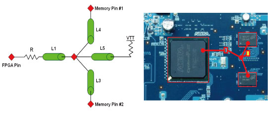
First, I organized the DDR2 bus signals into groups such as Address/Command Group, DATA Group, and Clock Group, and decided on the following topology for each group. Also, all DDR2 signals should be of equal length, and each terminating resistor and damping resistor should be installed as close to the pin as possible.
First is the Address/Command Group. Address/Command Group is the output signal from FPGA and the I/O standard is SSTL18-Class I. Install a damping resistor at the transmitting end of the FPGA and a Fly-By terminating resistor at the receiving end of the DDR2 SDRAM. Here, it is possible to replace the damping resistance on the transmitting end side of the FPGA with the internal resistance (On-Chip-Termination) that the FPGA has. The figure below (Fig.1) is an image diagram of the Address/Command Group when a damping resistor is placed externally.
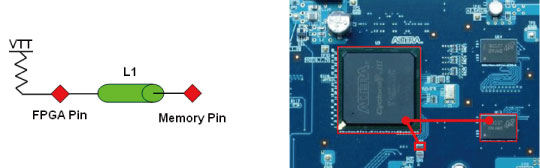
Next is the DATA Group. The DATA Group will be a bi-directional signal and the I/O standard will also be SSTL18-Class II. Since it is a bidirectional signal, Fly-By termination resistors are required on both sides of the FPGA and SDRAM. It is also possible to replace the Fly-By termination resistor on the DDR2 SDRAM side with the DDR2 SDRAM internal resistor (On-Die-Termination). The figure below (Fig.2) is an image diagram of the DATA Group when using the internal resistance of DDR2 SDRAM.
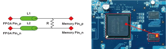
Next is the Clock Group. Clock Group is a differential signal and requires a 100 ohm differential termination close to the DDR2 chip.
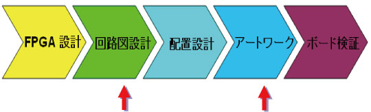
Based on such a determined topology, circuit input is performed, and then pattern design is performed. In the case of board design that realizes high-speed signals such as DDR2, it is necessary to incorporate design techniques that support high-speed signals in each phase of board design. However, with high-speed signals, many analog-like behaviors occur in the signals, and there are cases where past empirical rules are not enough to deal with them. Therefore, when it comes to designing high-speed signals, pre-verification by simulation is an important point in reducing backtracking man-hours.
Therefore, transmission simulation is basically performed twice, Pre and Post, as shown in the figure below (Fig.4). First, Pre-simulation is used to verify topology, component placement, and estimate resistance values.
Next, Post simulation verifies whether the design is appropriate after the implementation design. In simulation, not only can probes be placed anywhere, but values such as resistance and wiring length can be freely changed on the spot, enabling optimal board design. Therefore, our company used HyperLynx® and conducted a transmission simulation using IBIS. Cyclone III IBIS can be downloaded from Altera's website, but Quartus® II can also generate IBIS that reflects user settings (pin names, pin options, etc.).
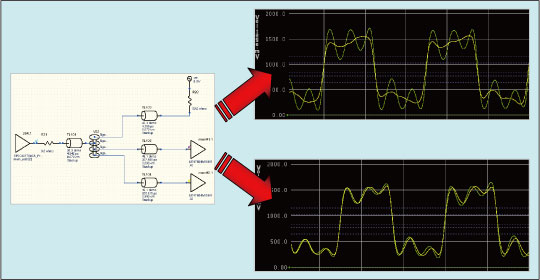
The figure below (Fig.5) is a simulation when two DDR2 SDRAMs are mounted on one FPGA. You can see that the waveform on the right is different from top to bottom. This results in a difference of 1mm (upper right) and 0.5mm (lower right) in each trace from the star via junction to the DDR2 SDRAM.
This error of 0.5 mm tends to be overlooked, but it can be improved by using a transmission simulator. Also, since the man-hours required for improvement are simulations, the values of resistors, capacitors, wiring lengths, etc. can be easily changed, so compared to debugging after the board has been created, it is much less.
By using a transmission simulator in this way, it is very easy to verify parts that were difficult to verify despite their importance. In addition, transmission simulation can verify not only the DDR2 SDRAM interface, but also the entire topology on the board, so we believe that problems caused by signal quality can be greatly reduced.
Sorry to keep you waiting! In the next issue, I will introduce the design and verification of USB 3.0. It's the last time. Do not miss it!
Part 1: Realization of USB3.0 interface using FPGA
Part 3: Design and verification of USB 3.0