- Semiconductor BusinessHOME
- Products and Services of Macnica,Inc.
-
technical information

-
Events and Seminars
- Handling Manufacturer
- Support
- Inquiry
- Click here to purchase products
- Semiconductor business e-mail magazine registration
![]()
![]() Narrow down by specifying conditions
Narrow down by specifying conditions
現在2183件がヒットしています。check

Introduction
hello! I'm Kurami.
A new question arose as I practiced production using FPGA.
The question is, "Will my design exceed the logic capacity of the FPGA I plan to use?"
After doing some research on this question, I came to the conclusion that
Unless you register your design in Quartus® Prime and compile the design, you cannot know how many logics your design has.
Therefore, I don't know whether it will exceed the logic capacity of the FPGA I plan to use.
However! !
There are several ways to estimate in advance, and I thought about various patterns.
1. If you improve the design you made before
2. When creating a new design
3. With Nios® II
4. When using SoC device
1. If you improve the design you made before
First, estimate the amount of logic for the new feature you want to add.
For example, if you add an 8-bit Counter circuit that continues to count up against CLK and a circuit that lights up an LED when the switch is pressed, you can imagine the following diagram. (Figure 1 )
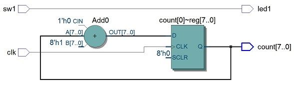
Visualize Figure 1 and approximate the approximate number of logic.
And the total logic count of the previous design plus the logic count of the added functionality is the approximate logic count of the improved design.
2. When creating a new design
Since there is no way to approximate this, you will not know unless you compile it with Quartus Prime once.
At that time, if you run a full compile, you can see the total logic count after placement and routing.
If you want to estimate the number of logics before placement and routing, check the number of logics after logic synthesis.
Let's take a look at the Compilation Report after doing Start Analysis & Synthesis in Quartus® Prime. (Figure 2)
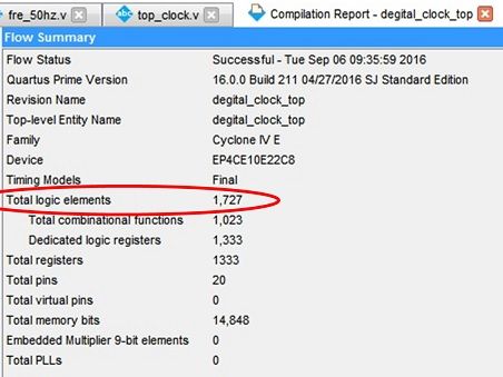
From Figure 2, we can see that there are 1727 Total logic elements before place and route.
Next, let's look at the Compilation Report after performing Start Compilation. (Fig.3)
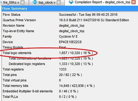
From Figure 3, we can see that there are 1657 Total logic elements after placement and routing.
In the Report after placing and routing, you can see what percentage of the logic capacity of the FPGA this design uses.
More questions arise here.
Why is the logic count different before and after place and route?
The logic count before placement and routing is the estimated logic count derived from the results of logic synthesis.
On the other hand, after full compilation, it is the result after all placement and routing has been completed, so you can check the number of logics actually used.
In this way, optimization such as register packing changes the number of logics after placement and routing. This time, the number of logics has decreased after full compilation, but please note that it does not always decrease.
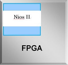
3. When using Nios II
I am also working on a production practice using Nios II, but how many logics will be when using this Nios II?
Nios II is ALTERA's soft core CPU.
This "soft" does not mean software. It is “soft” in the sense that it configures the CPU using FPGA logic.
The circuit of CPU is not included in FPGA from the beginning. When implementing Nios II in an FPGA, use the logic region of the FPGA.
Nios II is a CPU, so it doesn't work by itself.
Therefore, other necessary Peripheral IPs are incorporated, but FPGA logic is used for the number of logics of the IPs.
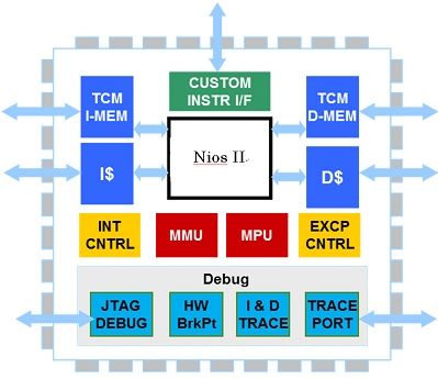
Also, a bus is needed to connect the Nios II to the IP, so bus capacity is also used.
Therefore, the logic capacity used when implementing Nios II on an FPGA is the total capacity when implementing Nios II = the capacity of Nios II alone + the capacity of the IP used + the capacity of the bus.
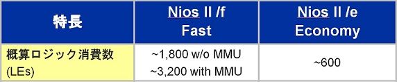
Table 1 is the logic estimation table for economy / fast on Nios II.
4. When using SoC device
This already has the [HPS] (vocabulary: Hard Processor System [HPS], a system that includes a CPU (ARM) and peripheral circuits) part built into the SoC device (Fig. 6).
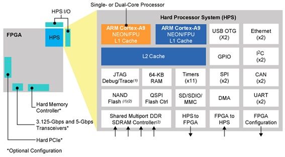
The [HPS] part is a fixed circuit and does not affect FPGA resources.
In other words, the amount of logic in an SoC device is determined only by the circuits implemented in the FPGA.
at the end
Now I know what kind of logic capacity FPGA to choose for my design.
Please take a look at the next article!