- Semiconductor BusinessHOME
- Products and Services of Macnica,Inc.
-
technical information

-
Events and Seminars
- Handling Manufacturer
- Support
- Inquiry
- Click here to purchase products
- Semiconductor business e-mail magazine registration
![]()
![]() Narrow down by specifying conditions
Narrow down by specifying conditions
現在2183件がヒットしています。check

Introduction
hello! I'm Kurami.
This time, I would like to deviate from the C language struggle for a moment and introduce Quartus® Prime's "Differences in usage between the RTL Viewer and Technology Map Viewer".
☆RTL Viewer
☆Technology Map Viewer
RTL Viewer
First, let me introduce a feature called the RTL Viewer.
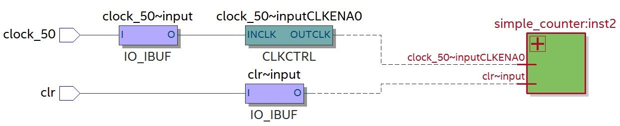
Use this function after Analysis & Elaboration.
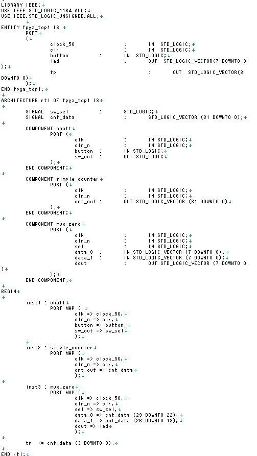
Figure 1 is an example of the HDL circuit created, and Figure 2 is the screen of the circuit displayed with the RTL Viewer.
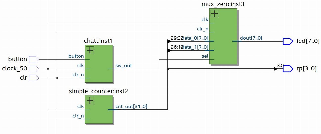
The green box represents the hierarchy, and you can view the inside of the logic block by clicking the + mark.
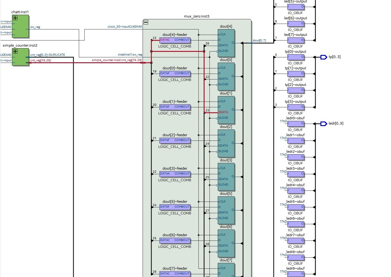
Figure 3 is a view after clicking the + mark of simple_counter in Figure 2.
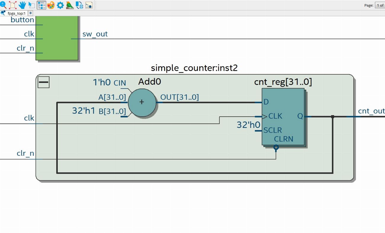
RTL constructs are I/O pins, registers, gates ( AND, OR, etc. ), operators ( adders, multipliers, etc. ), and so on.
Using the RTL Viewer in this way allows you to graphically check your design.
It can also be used for debugging, as it is displayed with optimizations such as connection checks and unconnected ports taken into consideration.
By using the RTL Viewer in my production practice, I was able to see the unconnected I/O that I thought was connected, which was very useful.
Technology Map Viewer
Next is an introduction to the Technology Map Viewer function. By launching this viewer, you can graphically check the circuit after logic synthesis and placement and routing. (Fig. 4, 5) Technology Map Viewer has Post-Mapping and Post-Fitting.
[Post-Mapping]
It is possible to check the circuit after logic synthesis with primitives such as logic elements, memory blocks, and I/O elements.
[Post-Fitting]
Post-place and route circuit also reflects optimizations performed during place and route.
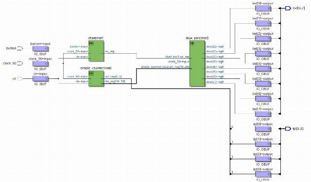
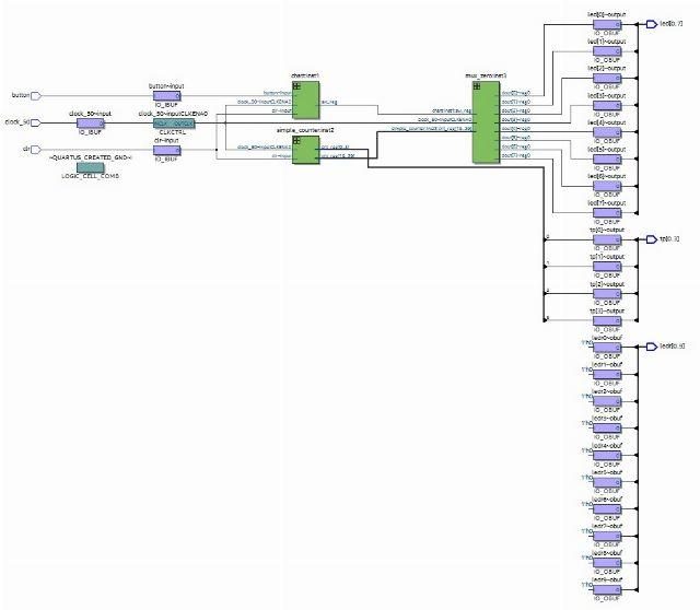
Figure 6 shows the inside of the logic block by clicking the + mark in the simple_counter hierarchy.
Blue boxes represent logic elements and green boxes represent registers.
You can see that what was displayed as Add (adder) in the RTL Viewer was actually configured as shown in Figure 6.
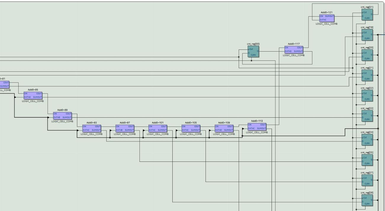
Elements of the Technology Map Viewer are I/O pins, logic cells (LCells), memory blocks, and so on.
With the Technology Map Viewer, you can see how Quartus® implemented your design using the logic cells inside the FPGA.
If you want to graphically check the final result after logic synthesis and placement and routing, it is convenient to use Post Fitting's Technology Map Viewer.
<Useful things to know>
1. In both RTL Viewer and Technology Map Viewer, move the cursor to a path and left-click to highlight the path. (Fig.7)
2. Filter allows you to pinpoint the selected part.
For example, if you want to pinpoint simple_counter, right-click simple_counter and select Filter. (Fig.8)
This time I chose Sources, which is one of the Filter functions.
This allows you to see what paths are connected to the selected input.
Summary
The difference in usage between the RTL Viewer and the Technology Map Viewer is as follows.
◎RTL Viewer
When you want to check the design graphically.
◎Technology Map Viewer
When you want to graphically see the design mapped to the logic cells inside the FPGA.
Using the above two functions is very convenient because you can smoothly check and debug the design!
Please take a look at the next article! !