- Semiconductor BusinessHOME
- Products and Services of Macnica,Inc.
-
technical information

-
Events and Seminars
- Handling Manufacturer
- Support
- Inquiry
- Click here to purchase products
- Semiconductor business e-mail magazine registration
![]()
![]() Narrow down by specifying conditions
Narrow down by specifying conditions
現在2189件がヒットしています。check
Expectations for charge pump ICs are increasing as power supply miniaturization and design efficiency are required. "What is a charge pump IC?" and "What are its advantages and limitations compared to other power supply ICs?"
Or there may be people who say, "I previously considered charge pump ICs, but they didn't meet the required voltage and current, so I left them out of the options."
Here, we will provide an easy-to-understand explanation of the basic features, benefits, and precautions to be taken when selecting charge pump ICs, whose choices have expanded significantly in recent years. We will also introduce the appeal of Analog Devices' lineup of "high voltage" charge pump ICs, as well as application examples for which they can be applied.
What is a charge pump IC?
A charge pump IC is a type of DC/DC converter that does not use an inductor. It adopts a method of outputting a voltage by transferring the electric charge and superimposing the voltage charged in the capacitor.
What features do they have compared to LDO regulators and switching regulators? The table below summarizes it.
| LDOregulator (three-terminal regulator) |
charge pump (aka: switched capacitor voltage converter) |
switching regulator (usinginductor)_ |
|
|
design complexity |
◎ |
〇 |
△ |
|
cost |
◎ |
〇 |
△ |
|
noise |
◎ |
〇 |
△ |
|
efficiency |
△ |
〇 |
◎ |
|
thermal considerations |
△ |
〇 |
◎ |
|
output current |
〇 |
〇 |
◎ |
|
Features |
Cannot boost/invert | Small input voltage/output current range (conventional) | Need to consider layout |
Similar to LDO regulators, no inductor is required. The big difference is that the LDO regulator does not have the function of boosting or inverting the voltage, but the charge pump IC can support boosting and inverting.
On the other hand, conventional charge pump ICs have a limited input voltage range and output current range. For this reason, until now, there have been many voices saying, "The voltage and current specifications do not match, and we have no choice but to choose a switching regulator that requires time and effort to design."
Advantages of charge pump ICs
Let's summarize the merits of charge pump ICs again. The following three points are typical advantages.
・The number of parts can be reduced with a simple circuit configuration.
In a basic circuit, the only peripheral parts required for a charge pump IC are a capacitor for charging power and an input/output capacitor. Since no inductor is required, a simple circuit configuration can be realized and the number of parts can be reduced.
・High efficiency regardless of load
Because the charge pump IC is PFM controlled, it can exhibit constant high efficiency under any load. On the other hand, switching regulators use PWM control, so efficiency drops especially at low loads.
・No magnetic flux generated, low output noise
Since no inductor is used, no magnetic flux is generated and output noise can be suppressed.
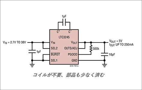
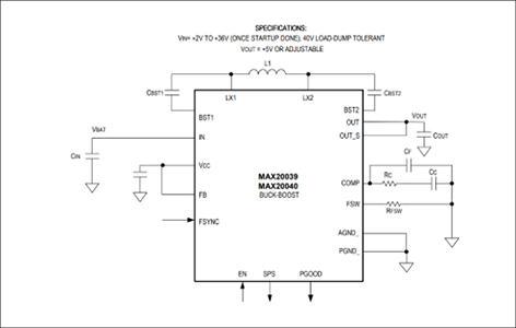
Below are two schematics. This is an example of configuring a buck-boost circuit with the same input/output conditions using a charge pump IC and a switching regulator. The example on the left is a charge pump IC, and the example on the right is a switching regulator.
As you can see at a glance, when configuring a circuit assuming similar input and output voltages, the charge pump IC has no inductor and few peripheral components, so the circuit is overwhelmingly simple. Compared to a switching regulator, it can be designed much easier.
Disadvantages and Limitations - Points to note when choosing
On the other hand, what are the disadvantages and limitations of charge pump ICs? In general:
・Unsuitable for cases with large voltage and current
Since energy is stored in a capacitor to operate, until now it could only handle relatively small voltages and currents.
・Large ripple voltage
Since it does not use an inductor, the ripple voltage at the output is larger than that of a switching regulator.
Due to these characteristics, charge pump ICs have been adopted mainly for power consumption and noise sensitive applications that require low power and small size.
<Example>
-LED power supply
-High voltage power supply for LCD
-mobile phone
-remote control
-Small IoT devices
Under these circumstances, in recent years Analog Devices has released high-voltage charge pump ICs that can handle higher voltages and currents than before. A high voltage charge pump IC would greatly expand the available applications.
Appearance! High voltage charge pump IC
From here, let's introduce the high-voltage charge pump IC"LTC32xx series" from Analog Devices.
The input voltage of general charge pump ICs is about 12V, but the LTC32xx series supports input voltages up to 55V. Another big attraction is that it supports an output current of up to 500mA.
In the past, even in cases where voltage and current were insufficient, it became possible to add a charge pump IC as a new option. It can be said that it is truly an epoch-making lineup.
We offer a wide variety of products as shown below.
| Vinmin(V) | Vinmax(V) | Iout | Functions | ||
| LTC3255 | 4 | 48 | 50mA | Buck | |
| LTC3256 | 5.5 | 38 | 350mA | Buck + Buck LDO | |
| ✅ | LTC3260 | 4.5 | 32 | 100mA | Inverting → independent positive and negative LDOs |
| LTC3261 | 4.5 | 32 | 100mA | reversal | |
| ✅ | LTC3245 | 2.7 | 38 | 250mA | Buck-boost |
| LTC3246 | 2.7 | 38 | 500mA | Buck-boost | |
| LTC3265 | 4.5 | 32 | 100mA | Boost & inversion → independent positive and negative LDO | |
| ✅ | LTC3290 | 4.5 | 55 | 50mA | Tracking mode with boost + fixed offset |
✅: Automotive products (AEC-Q100 certified)
A common attraction for the entire series is:
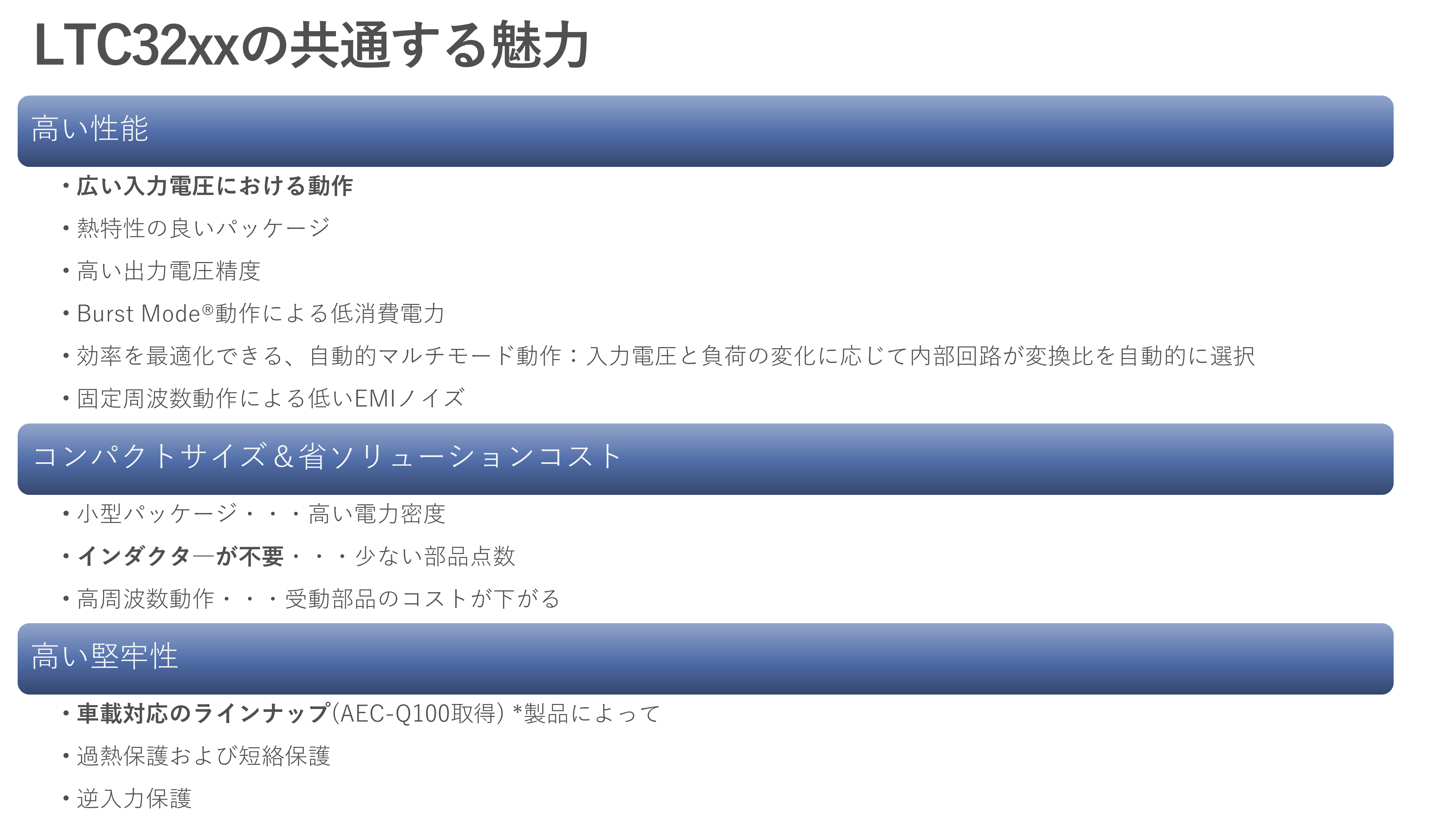
In terms of performance, the most noteworthy feature is the operation over a wide range of input voltages. Of course, the unique merit of a charge pump IC, which does not require an inductor, contributes to miniaturization and the reduction of parts. An automotive-grade lineup is also provided to meet high robustness requirements.
LTC32xx series lineup introduction
Here, we will introduce four carefully selected types from our extensive lineup.
[LTC3256] Dual Output Step-Down Charge Pump with Watchdog Timer
The LTC3256 is a dual output step-down charge pump IC with a watchdog timer that allows flexible system design. It supports an input voltage of up to 38V, and the total output current of the two systems is 350mA.
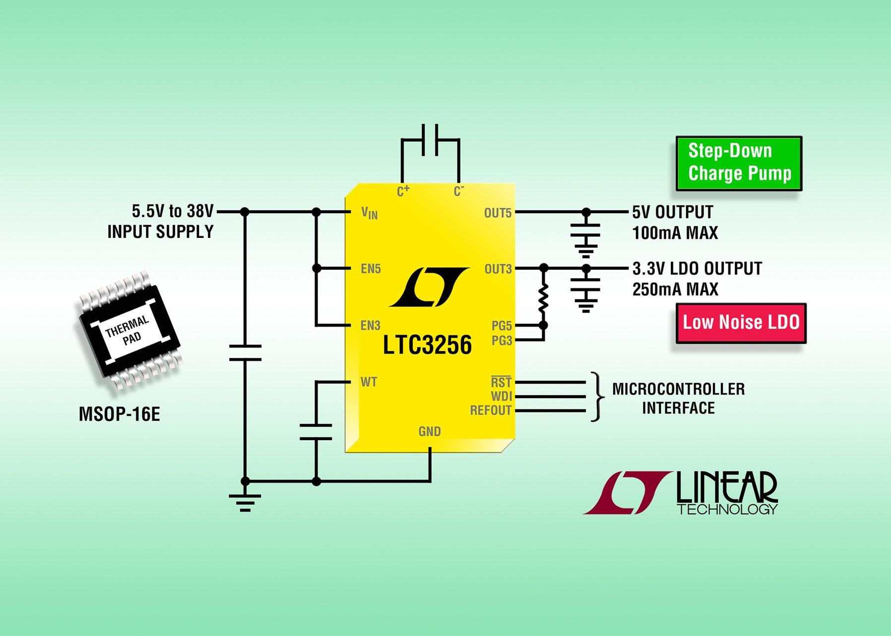
Main features
■ 2 fixed outputs
-Buck charge pump (5V)
-Low noise output (3.3V) via LDO
■ Input voltage range: 5.5V to 38V
■ Output current: Total 350mA
-5V output: 100mA max
-3.3V LDO output: up to 250mA
■ Low quiescent current
- No-load quiescent current: 20μA total for 2 channels
- Shutdown: 0.5μA
■ 1.1V reference output for system diagnostics
■ Input current control for low noise
■ With programmable watchdog timer
[LTC3260] Low-Noise Dual-Supply Inverting Charge Pump (For Automotive)
The automotive-grade LTC3260 is a charge pump IC that can generate independent positive and negative voltages from a single input voltage system. It can output up to 50mA of current from each channel and supports a wide input voltage of up to 32V.
Recommended applications include generating ± power supplies for op amps. In particular, it will have a high degree of contribution in industrial and measurement equipment that requires low-noise operation of operational amplifiers.
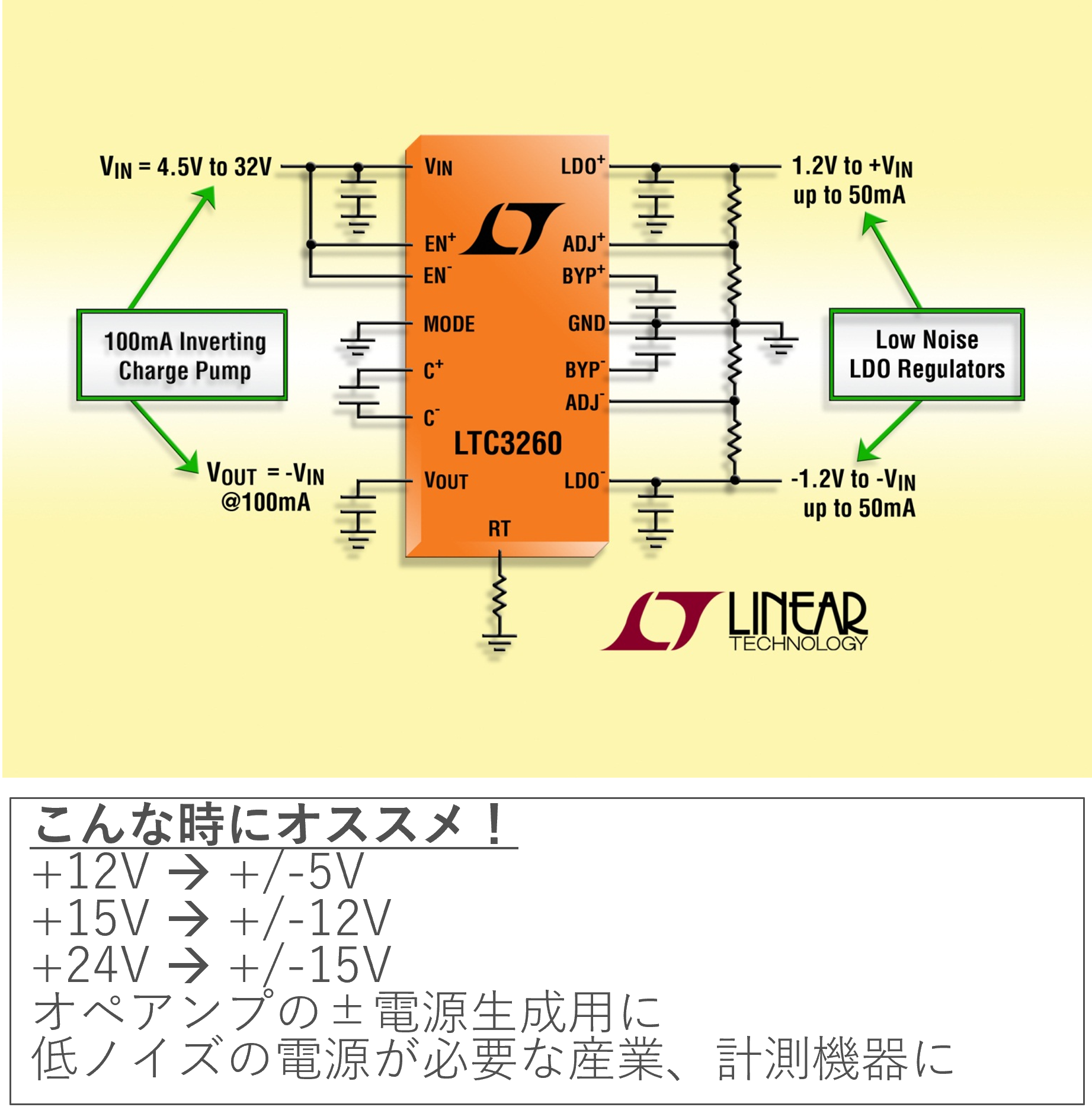
Main features
■ Input voltage range: 4.5V to 32V
■ Negative voltage generation by inverting charge pump
■ Independent positive and negative voltage LDOs with low noise (up to 50mA for each channel)
■ Quiescent current in Burst Mode® operation: 100 μA total
■ Resistor-configurable oscillator frequency: 50kHz to 500kHz
■ Stable operation with ceramic capacitors
[LTC3245/6] Wide input voltage buck-boost charge pump 250mA/500mA (automotive compatible)
The automotive-grade LTC3245 /6 is a buck-boost charge pump with a very wide input voltage range of 2.7V to 38V. High conversion efficiency and low no-load quiescent current are also notable features.
Recommended applications include automotive and industrial applications where board space is limited and low power consumption is required. For example, it is also ideal for power supply of in-vehicle ECU/CAN transceiver.
Main features
■ Wide input voltage range:2.7V – 38V
■ Output voltage = Fixed 3.3V, 5V / Arbitrary adjustment
■ Output current (IOUT): Maximum 250mA
■ No-load quiescent current= 15uA, 2uA(at shutdown) *For LTC3246
■ Efficiency at12Vinput5V output: 81%
■ Low noise due to fixed frequency operation
■ Package with improved thermal characteristics
■ Overheat protection and short circuit protection
■ Operating temperature: up to 150℃
[LTC3290] High Voltage Boost Charge Pump (For Automotive)
Finally, I would like to introduce "LTC3290". This step-up charge pump IC is suitable for automotive applications and can withstand the maximum input voltage of 55V in this series.
Reverse input is also a concern for high voltage applications, and the LTC3290 features reverse input protection down to-55V, making for a very robust power supply design. .
This IC is ideal for generating high-voltage boosted power supplies that require high efficiency, and can be used in a wide range of applications, both in-vehicle and industrial machinery. For example, it is an easy-to-use product for high-voltage high-side Nch-FET drivers.
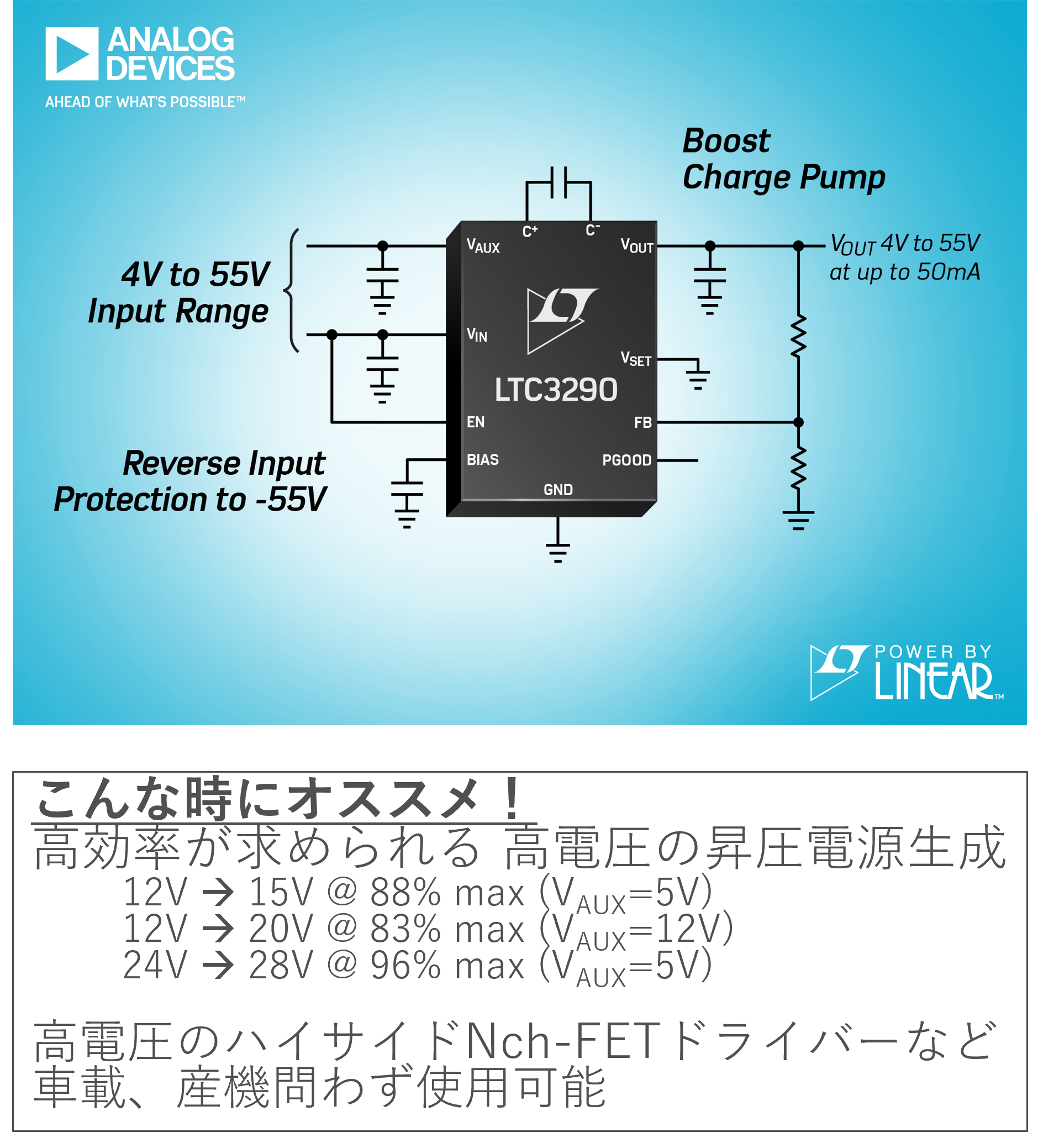
Main features
■ Wide input voltage range: 4.5V to 55V Vin/Vaux
■ Reverse input protection function up to –55V
■ Separate input power supply that achieves high efficiency boost rate
■ Output current (Iout): Maximum 50mA
■Vin quiescent current: 15µA
■Vaux quiescent current: 1µA
■ Stable operation with ceramic capacitors
■ Configurable tracking mode
-Can be regulated at voltages where the output voltage is higher than the input voltage by a fixed value
We picked up and introduced four types from the LTC32xx series. All of them cover a wide range of input voltages and can flexibly handle large current outputs.
A high-voltage charge pump IC can now handle cases that were previously only possible with switching regulators. Please take this opportunity to add a high-voltage charge pump IC to your selection.
Application example
・Transceiver in automobile ECU
・Portable POS terminal

Click here to purchase products
Click here for manufacturer site/other related links
Inquiry
If you have any questions regarding this article, please contact us below.
Analog Devices Manufacturer Information Top
If you want to return to Analog Devices Manufacturer Information Top, please click the button below.