
![]()
![]() Narrow down by specifying conditions
Narrow down by specifying conditions
現在1888件がヒットしています。check


hello.
My name is Intel F. Hanako and I provide technical support for Intel® FPGA at Macnica.

This time, "Light blinking with Intel® FPGA"
Introducing the Nios® IIsoft-core processor!
[Related Information] Nios® II Processor on Intel® FPGA
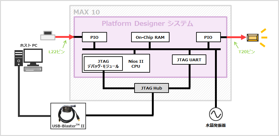
The LED lights only when the push button on the board is pressed, and turns off when the push button is released.
This operation is performed by the Nios ® II soft-core processor (hereafter referred to as Nios ® II).
★ Check out the video of the L flash that will be held this time

* Please see this content for how to make the LED blink only with the logic circuit of the HDL language.
■ Things to prepare
This development environment uses these.
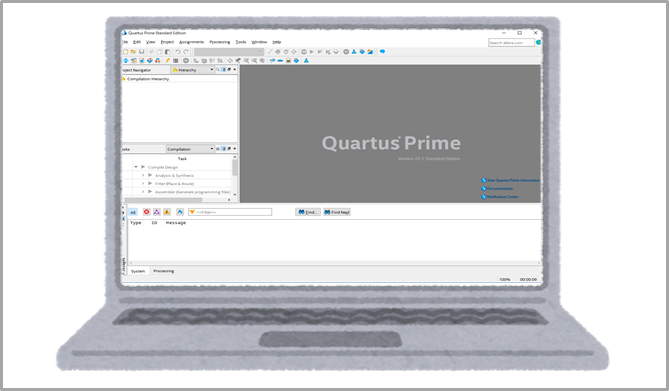
Quartus® Prime Standard Edition
or Lite Edition (free)
&
Nios II Software Build Tools for Eclipse (*)
Questa* - Intel® FPGA Edition
or
Questa - Intel FPGA Starter Edition (Free)
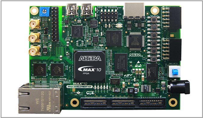
MAX® 10 FPGA Development Kit
Please contact us for consideration and purchase.
(Also available at Macnica Mouser.)
* To use Nios ® II Software Build Tools, Windows Subsystem for Linux and Eclipse must be installed.
Please see this content for details.
■ Development board connection configuration
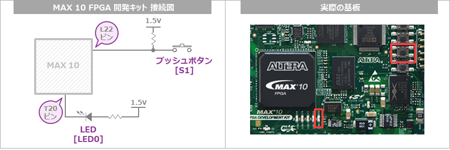
The pushbutton [S1] and LED [LED0] are connected on the board as shown.
(* In addition, push button [S2] is used as a system reset signal.)
"The LED lights when the push button is pressed, and the LED goes off when the push button is released."
To make Nios ® II do this, there are two main tasks.
✔ Embed Nios ® II in FPGA
✔ Create a program (C language) to be executed by Nios ® II
This LED blinking operation can be easily written in HDL language, but let's use Nios ® II this time.
(This is the first step toward system development using Nios ® II!)
■ Work steps
In this sample project, we will do the following:
- Designing Nios® II and Peripheral Circuits with Platform Designer
- Finalize your FPGA design
- Do RTL level simulation
- set constraints
- to compile
- Validate timing
- Download hardware design to FPGA
- Running Software on Your System with the Nios II Software Build Tools for Eclipse (Go to Part 2)
- Incorporating the Nios® II Boot Program into the FPGA's On-Chip Memory (Go to Part 2)
For shortcuts to each task, click the items above or on the left side of the screen.
For the general flow of development, see Intel® FPGA Development Flow.
1. Design Nios® II and peripheral circuits with Platform Designer
1-1. Quartus® Prime project creation
Select the Quartus ® Prime menu below to create a project.
File➤New Project Wizard
Here, set the project name and top level entity name to presspb_led_nios2.
Target device is MAX ® 10 FPGA Development Kit 10M50DAF484C6GES Choose.
1-2. Create a Nios® II system
Quartus ® From the Prime menu below Platform Designer Start Nios ® II Build the processor and peripheral circuits.
Toolsmenu➤ Platform Designer
The Nios ® II system configuration created in this sample project is shown below.
Also, the Nios ® II boot memory and execution memory are assumed to be On-Chip RAM.
1-2-1.
Add a Nios ® II Processor.
Select Nios II Processor from the IP Catalog in the upper left corner of Platform Designer, and select Nios II/e from the core type.
(It will be added when you click the [Finish] button.)
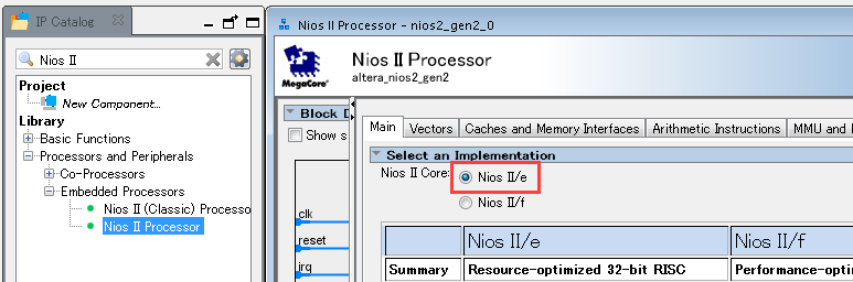
You'll see an error in the Messages tab, but let's continue for now.
1-2-2.
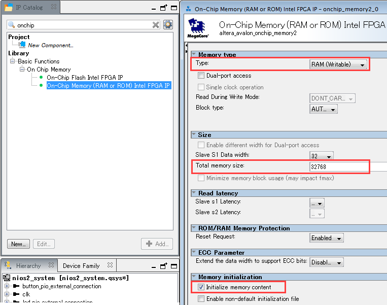
Add On-Chip Memory.
Similar to Nios ® II, select the On-Chip Memory (RAM or ROM) Intel FPGA IP from the IP Catalog and configure it as shown below.
Otherwise, leave the defaults and click the [Finish] button.
1-2-3.
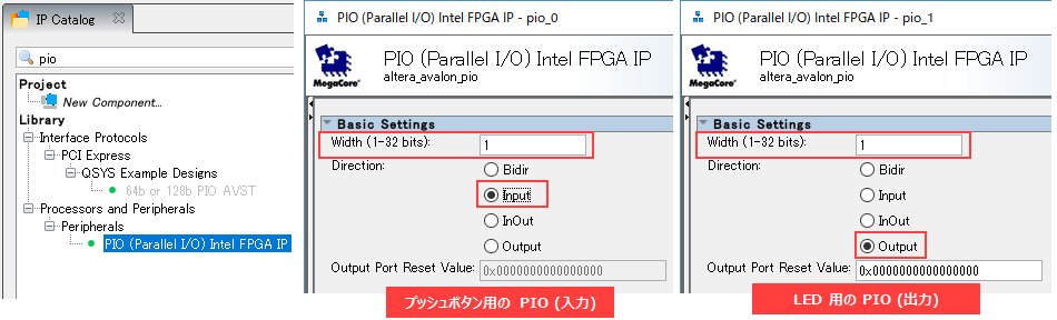
Add PIOs.
Select the PIO(Parallel I/O)Intel FPGA IP from the IP Catalog and specify the bus width and input/output attributes.
Create a PIO for the push button and a PIO for the LED.
1-2-4.
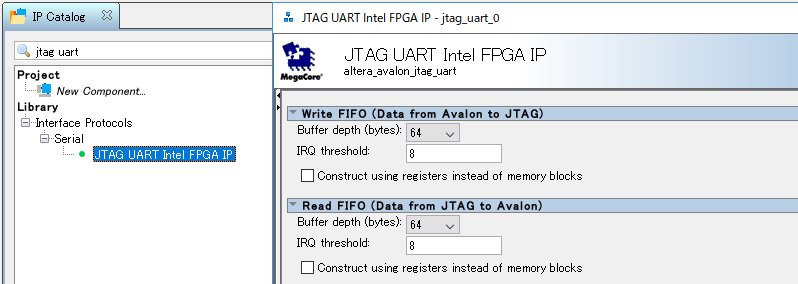
Add JTAG UART.
In order to debug printf, we will create a JTAG UART Intel FPGA IP that communicates via UART with a PC via the JTAG interface (via USB-Blaster™ II).
Click the [Finish] button with the default settings.
1-2-5.
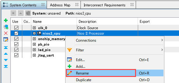
Rename each component.
Rename in the Name column of the System Contents tab.
The sample design follows the table below.
| Name before change | Name after change |
| nios2_gen2_0 | nios2_cpu |
| onchip_memory2_0 | onchip_memory |
| pio_0 | pb_pio |
| pio_1 | led_pio |
| jtag_uart_0 | jtag_uart |
1-2-6.
Click the white circle in the Connections column to change it to a black circle (connection) and connect each component.
In the sample project, connect as shown below.
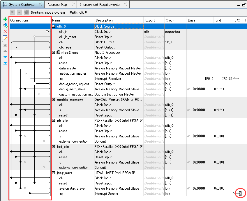
1-2-7.
Connect the interrupt port.
Connect Interrupt Sender of JTAG_UART and Interrupt Receiver of Nios ® II Processor as shown above.
The value indicates the priority, but since there is only one interrupt this time, leave it at 0.
1-2-8.
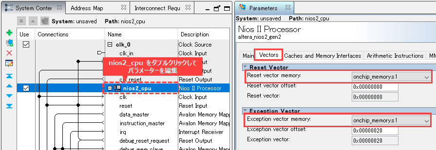
Sets the Nios ® II Reset Vector / Exception Vector.
In the sample project, the Nios ® II boot memory and execution memory are set to On-Chip RAM (onchip_memory).
Set the Nios ® II Reset Vector and Exception Vector as shown below.
1-2-9.
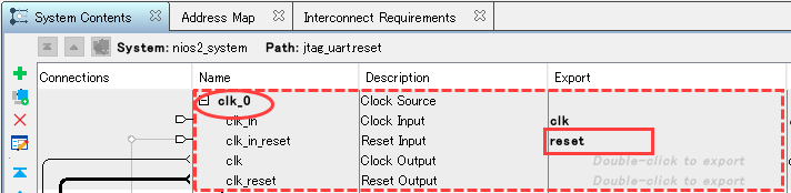
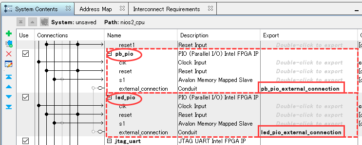
Export the reset signal and PIOs outside the Nios ® II system.
Double-click the Export column of clk_in_reset of clk_0 to create a port.
Double-click the Export column of the external_connection for pb_pio and led_pio respectively to create the ports.
1-2-10.
Set the base address so that it does not overlap.
By executing the menu below, the base address is automatically set to an appropriate value.
Platform DesignerSystemmenu➤ Assign Base Address
1-2-11.
Your Nios ® II system is now complete.
Save the qsys file with a name in the Filemenu➤ Save As….
For the sample project, save it as nios2_system.qsys.
1-2-12.
Generate a module for the Nios ® II system.
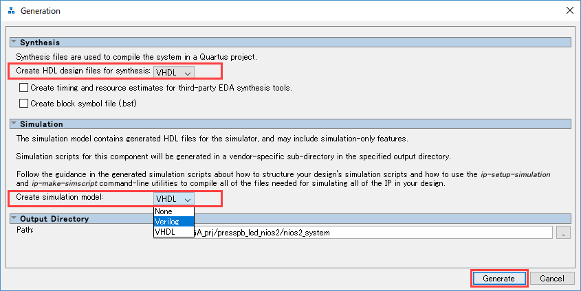
|
[Synthesis] Create HDL design files for synthesis: |
Specifies the HDL language for logic synthesis when compiling with Quartus ® Prime. |
|
[Simulation] Create simulation model: |
Specify the HDL language of the model for simulation. |
|
[Output Directory] Path: |
Specifies the folder in which to generate the files. (Leave the default for the sample project.) |
Click the [Generate] button at the bottom right of the Platform Designer screen to generate the module.
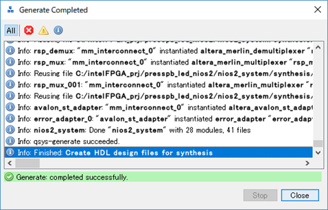
After file generation is complete and the Generate Completed window is closed with the [Close] button, click the [Finish] button at the bottom right of Platform Designer to close Platform Designer.
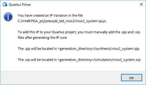
The following window will be displayed. Check the contents and click the [OK] button.
(* This description will be performed in step 2-2.)
2. Complete FPGA design
2-1. Implement Nios® II system in user design
Incorporate the system module created in Platform Designer into the top-level HDL design.
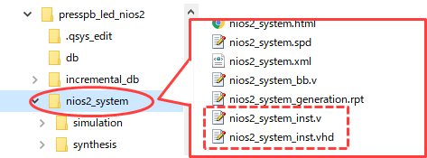
There is an instance auxiliary file (*_inst.vhd / *_inst.v) in the folder where the Nios II system created with Platform Designer is saved so that it can be easily incorporated into the top-level hierarchical design. let it complete.
For example:
![]() VHDL top design sample description
VHDL top design sample description ![]() Verilog HDL Top Design Sample Description
Verilog HDL Top Design Sample Description
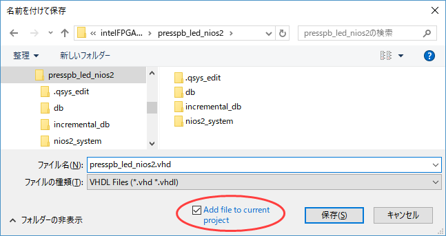
Name the file and save it with Filemenu➤ Save As….
For this example project, save as presspb_led_nios2.vhd / presspb_led_nios2.v.
2-2. Register design
Register your HDL design and Nios ® II system in a Quartus ® Prime project.
Projectmenu➤ Add/Remove Files in Project
Register your top-level HDL design (presspb_led_nios2.vhd or presspb_led_nios2.v) and the .qip file for your Nios ® II system.
Similarly, let's register the Nios ® II system .sip file for later RTL simulation with NativeLink.
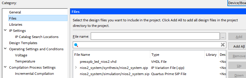
note that
The .qip is in the folder for modules/synthesis created in Platform Designer.
The .sip is in the module folder/simulation created in Platform Designer.
<Related FAQ> What kind of file is a .sip file?
▲ Return to the list of work steps
2-3. Elaboration execution
Go to Processingmenu➤Start➤Start Analysis & Elaboration.
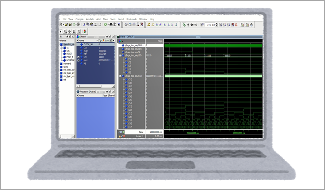
3. Do RTL level simulation
Run RTL simulation to check operation.
Refer to the table below and refer to the information depending on what you want to simulate.
|
Contents of the simulation to be carried out |
Reference information |
| Simulate only the hardware behavior of the entire project design, excluding the Nios ® II software behavior | |
| Simulate Nios ® II software behavior using only Platform Designer's system module | |
| Simulate the entire project design including Nios ® II software behavior |
This sample project is
Third ″Nios ® IISimulate the entire project design including the software behavior of″ I will guide you through the flow.
3-1. Create a software project
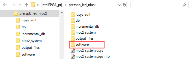
Quartus in advance ® Inside your Prime project folder, software project Manually create a workspace (folder) for
For the sample project, create a software folder.
Start the Nios II Software Build Tools for Eclipse (hereafter, Nios II SBT) from the Tools menu of Quartus ® Prime.
Tools menu ➤ Nios II Software Build Tools for Eclipse
<Caution>
To use Nios II SBT in Quartus ® Prime Standard Edition 19.1 or later environment, please install WSL and Eclipse in advance. For details, please see the content below.
(Install Windows Subsystem for Linux and Eclipse)
In the Workspace column of the launched Workspace Launcher, specify the workspace folder software created earlier.
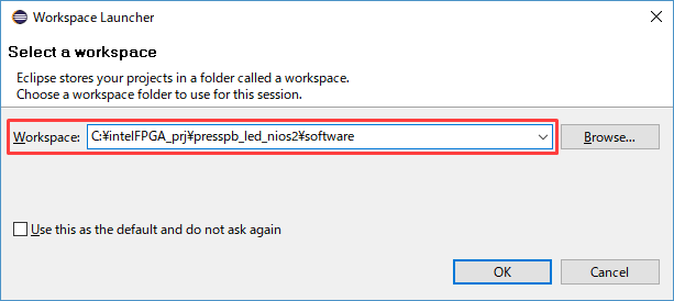
The Nios II SBT will start.
From the Nios II SBT menu below, start the wizard for creating a project.
File menu ➤ New ➤ Nios II Application and BSP from Template
Specify:
|
item name |
Settings |
|
SOPC Information File name |
nios2_system.sopcinfo (Operation 1. The embedded system hardware information generated by Platform Designer is Point your browser to the system definition file .sopcinfo. ) |
|
Project name |
soft_test |
|
Templates |
Blank Project |
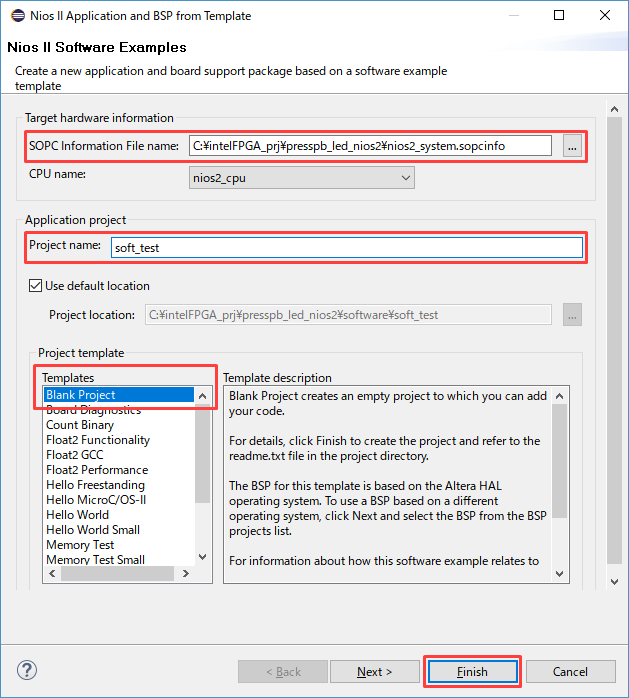
Click the [Finish] button.
A new project is created and soft_test and soft_test_bsp are added inside the Project Explorer tab.

3-2. Create C source code to run on Nios® II
Right-click the soft_test folder on the Nios II SBT and select New ➤ Source File.
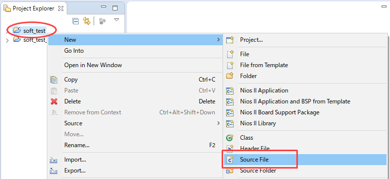
In the New Source File window, specify the Source folder and enter the file name of the C source code to be created in Source file.
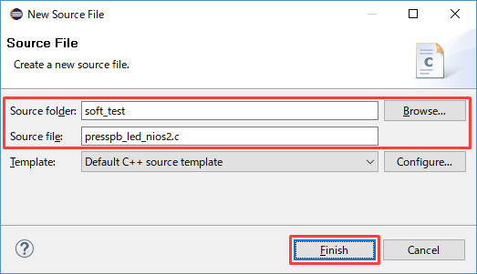
Click the [Finish] button.
Write the following code in the editor displayed on the main screen.
#include "sys/alt_stdio.h" #include "system.h" int main() { alt_printf("Hello from Nios II !!"); while(1) { int reg; reg = *(volatile unsigned char *) PB_PIO_BASE; *(volatile unsigned char *) LED_PIO_BASE = reg; } return (0); } ![]() presspb_led_nios2.c sample description
presspb_led_nios2.c sample description
After completing the description, save the file with Filemenu➤Save.
3-3. System settings
Start the BSP Editor from the menu below.
Right-click the ″software project name″_bsp folder ➤ Nios II➤ BSP Editor
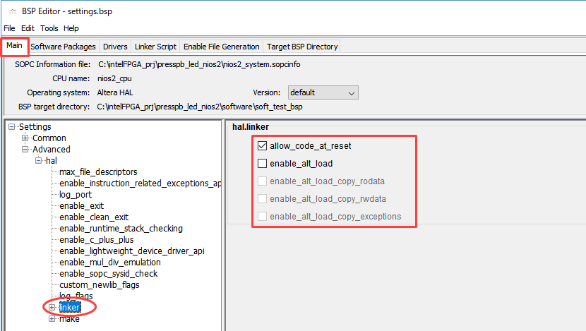
In the sample project, the Nios ® IIboot memory and execution memory are both On-Chip RAM.
Set as follows.
[Main tab]
・Settings ➤ Common ➤ Hal
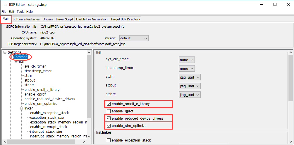
Leave everything else as default.
[Note]
The “enable_sim_optimize“ option has the effect of reducing the time to run the main() function during simulation.
After the simulation work is finished, turn it off. Code built with this option checked cannot be used in a real application.
・Settings ➤ Advanced ➤ hal.linker
[Linker Script tab]
Make .bss, .heap, .rodata, .rwdata, .stack, .text all On-Chip RAM (onchip_memory).
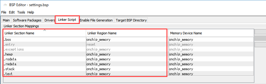
Then click the Generate button.
After confirming the log of ″INFO: Finished generating BSP files.″, close the BSP Editor with the [Exit] button.
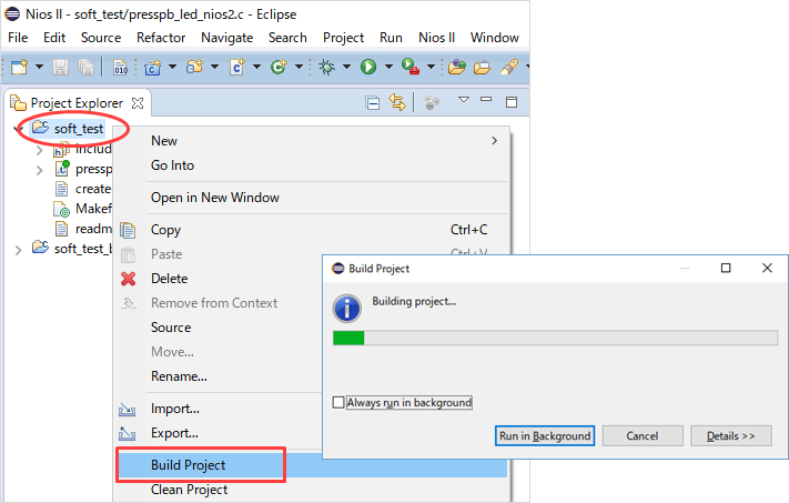
3-4. Build the software project
Select the application project (folder without _bsp) with the mouse.
Right click➤ Build Project to run the build.
3-5. Generate software Hex file
In Nios ® II SBT, right-click the application project (folder without _bsp) and select to generate the HEX file of the software from the menu below.
Make Targets➤ Build...➤ mem_init_generate➤ Click the [Build]button
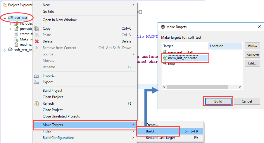
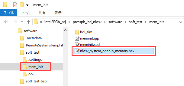
You can confirm that *_onchip_memory.hex has been generated in the \\<application project folder>\mem_init folder.
Close the screen with Nios II SBT's Filemenu➤Exit.
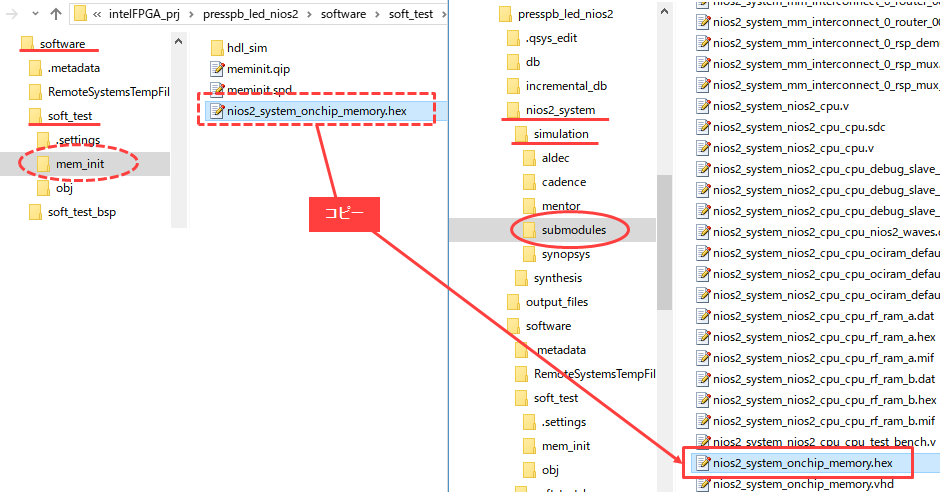
3-6. Copy *_onchip_memory.hex file
Copy the *_onchip_memory.hex file generated earlier to the folder where the simulation model is saved.
<Quartus Prime project>/<Platform Designer folder>/simulation/submodules
Copy to
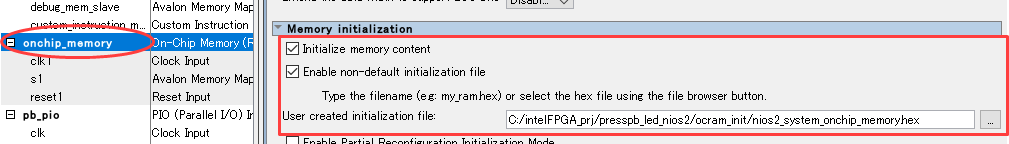
If the initial value setting of the on-chip memory created with Platform Designer is not the default setting as shown in the figure below,
Copy the generated *_onchip_memory.hex file to the specified folder,
If the file name is different, change the *_onchip_memory.hex file to the specified file name.
3-7. NativeLink simulation settings
Build an environment to run NativeLink on Quartus ® Prime.
Please refer to "Setting the environment" in this content and set it.
Set up NativeLink simulation from the Quartus ® Prime menu below.
Assignmentsmenu➤Settings➤EDA Tool Settings➤Simulation
|
item name |
Settings |
| Tool name | EDA tools used for simulation |
| Format for output netlist |
Select Verilog HDL (Specify Verilog here, even if it is a VHDL design.) |
| Output directory | Default (simulation/<tool_name>) |
| Compile test bench |
Setting up the original testbench
Please refer to the work flow “3. Register the testbench in NativeLink settings”. ) |
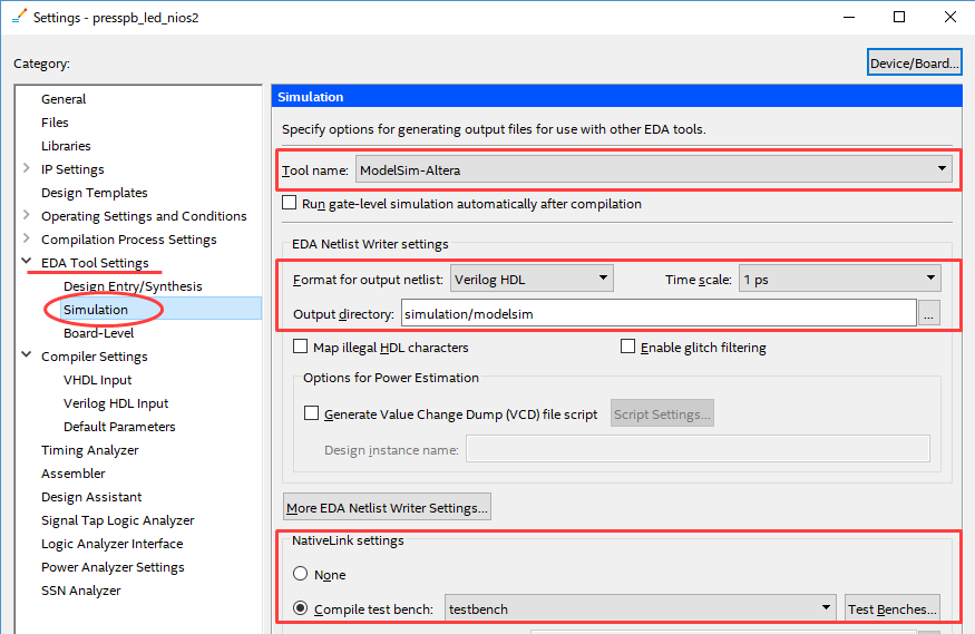
Close each window with OK.
3-8. Execution of function simulation with NativeLink
Click Toolsmenu➤ Run Simulation Tool➤ RTL Simulation.
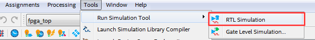
* Analysis & Elaboration or Analysis & Synthesis or Fitter process must be executed in advance to execute RTL Simulation.
However, do not run Start Compilation (Processing menu). The EDA Netlist Writer was automatically run.
It may not generate scripts for successful RTL Simulation.
If you have run a full compile, run Analysis & Elaboration or Analysis & Synthesis again, or run the Fitter again.
Do RTL Simulation.
Waveforms are displayed in the Wave window.
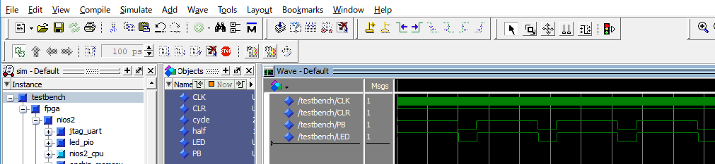
After confirming that the expected behavior is achieved, exit the simulation and Questa - Intel FPGA Edition.
Questa - Intel FPGA Edition Simulate menu ➤ End Simulation, File menu ➤ Quit
Then change the Tool name back to <none> in the Quartus Prime Assignments menu ➤ Settings ➤ EDA Tool Settings ➤ Simulation.
[reference]
When simulating with ModelSim (including Intel FPGA Edition) without using NativeLink
Customize the simulation script file msim_setup.tcl in the Platform Designer generated folder.
/<Nios II system folder>/simulation/mentor/msim_setup.tcl
Please refer to the following contents for editing and work flow of msim_setup.tcl.
4. Set constraints
4-1. Setting pin assignment
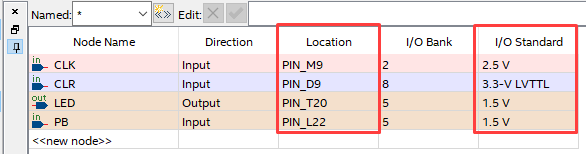
Launch the Quartus ® Prime Assignments menu ➤ Pin Planner to assign pins in your design to the FPGA.
For the MAX ® 10 FPGA Development Kit, set the pins as follows:
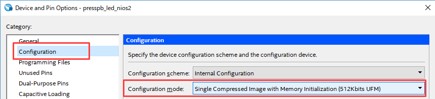
4-2. Select configuration mode
Specify the configuration mode in the Quartus ® Prime Assignmentsmenu➤ Device➤ Device and Pin Options.
For this example project, select Single Compressed Image with Memory Initialization.
4-3. Setting Timing Constraints
Create timing constraints for your project design.
Since the sample project is designed to operate with a 50MHz clock, create an SDC that describes the clock definition command,
Add to the project.
The SDC for the Nios ® II system is the SDC file automatically generated when registering the qip file (step 2-2).
Applied to the Timing Analyzer (Assignments menu ➤ Settings).
Although timing constraints on user I/O pins are inherently required,
In this sample project, both the input signal (when a person presses and releases the push button) and the output signal (LED turns on/off) are very slow, so I/O timing constraints are omitted here.
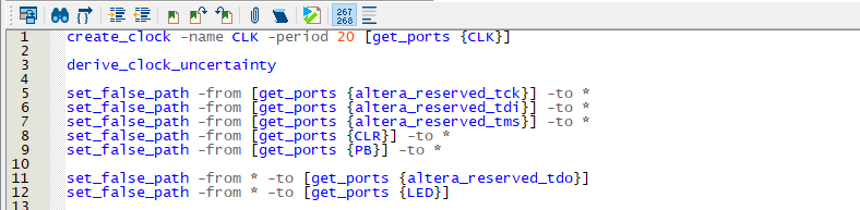
Create an sdc file of the user circuit and register it in the project.
5. Compile
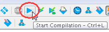
Execute compilation using the following menu.
Processing ➤ Start Compilation
Logic synthesis and placement and routing are executed, and program data to be written inside the FPGA is generated at the same time.
After compiling, examine the generated compilation report.
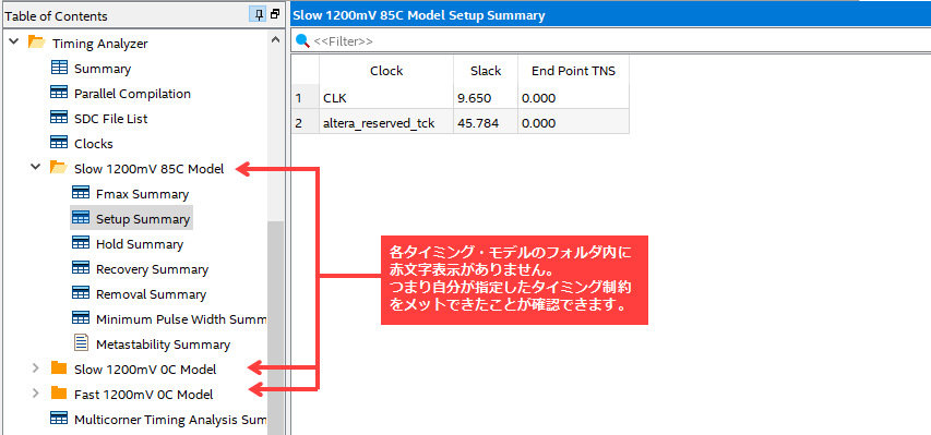
6. Validate timing
Expand the Timing Analyzer folder in the compilation report to verify timing.
You can confirm that each timing model has cleared the clock frequency constraints.
7. Download hardware design to FPGA
Connect the MAX ® 10 FPGA Development Kit to your computer with a mini-USB cable.
Connect the power cable and apply power to the board (On).
[Reference information] Installing the USB-Blaster II driver
Quartus ® From the Prime menu below Programmer Start the
Tools➤ Programmer
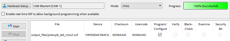
Select USB-Blaster II from Hardware Setup
Compiling MAX ® 10 generates two types of write files (.sof / .pof).
First of all, we will implement the hardware circuit on the actual machine and debug the software operation, so download the SOF file.
In the sample project, set presspb_led_nipos2.sof and click the Start button.
Data transfer is complete when Programmer's Progress bar reaches 100% (Successful).
▲ Return to the list of work steps
The hardware circuit data has been transferred to the FPGA, but there is still no program for the internal Nios ® II to execute.
So, of course, pressing the push button [S1] on the development board does not turn on the LED.
Next, let's develop software to run on Nios ® II.
The first L blinking on Intel FPGA Nios® II! (Part 2)
Click here for recommended articles/materials
Getting started with Intel FPGA
The first L blinking with Intel FPGA!
The first LED blinking on the Intel FPGA Nios® II! Part 1
The first LED blinking on the Intel FPGA Nios® II! Part 2
Boot Nios® II with FPGA's on-chip memory
Boot Nios® II with UFM in MAX® 10
Nios® II Processor on Intel® FPGA
Intel® FPGA Development Flow/Top Page
Click here for recommended seminars/workshops
"Nios® II Introductory Edition Trial" released in video!