
![]()
![]() Narrow down by specifying conditions
Narrow down by specifying conditions
現在1888件がヒットしています。check


hello.
My name is Intel F. Hanako and I provide technical support for Intel® FPGA at Macnica.
This page introduces how to put Nios® II into Intel FPGA and make it blink.

So far, we have performed operations 1 to 7 of the following. (Please see this content for the contents so far.)
This time (Part 2) will introduce operations8 to 9 as a sequel.
1. Design Nios® II and peripheral circuits with Platform Designer
2. Complete FPGA design
3. Do RTL level simulation
4. Set constraints
5. Compile
6. Validate timing
7. Download hardware design to FPGA
8. Nios II SBTto run software on the system
9. Incorporate the Nios® IIboot programinto the FPGA's on-chip memory
From here on, we assume that you have already created a software project in Nios II SBT.
If you have not yet created a software project
The first L blinking on Intel FPGA Nios® II! Part 1, please perform operation 8 onwards after performing operation 3-1 to operation 3-3.
Also, later in the page, you'll find a useful
We also show you how to update quickly. Must see!
8. Nios II SBT to run software on system
Run the software program built with the Nios II SBT on the target system.
* To run the software, the hardware image (*.sof) must be programmed in the FPGA in advance.
Please refer to "7. Download hardware design to FPGA" in this content for programming method.
Start the Nios II Software Build Tools for Eclipse (hereafter, Nios II SBT) from the Quartus ® Prime menu below.
Tools menu ➤ Nios II Software Build Tools for Eclipse
<Caution>
To use Nios II SBT in Quartus ® Prime Standard Edition 19.1 or later environment, please install WSL and Eclipse in advance.
For details, please see the content below.
(Install Windows Subsystem for Linux and Eclipse)
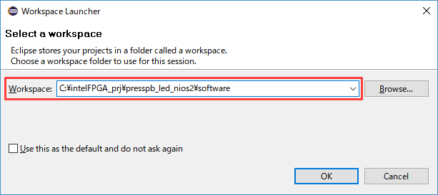
Specify the workspace folder with the software project in the Workspace field of the launched Workspace Launcher.
In the sample project:
\\<Quartus Prime project>\software
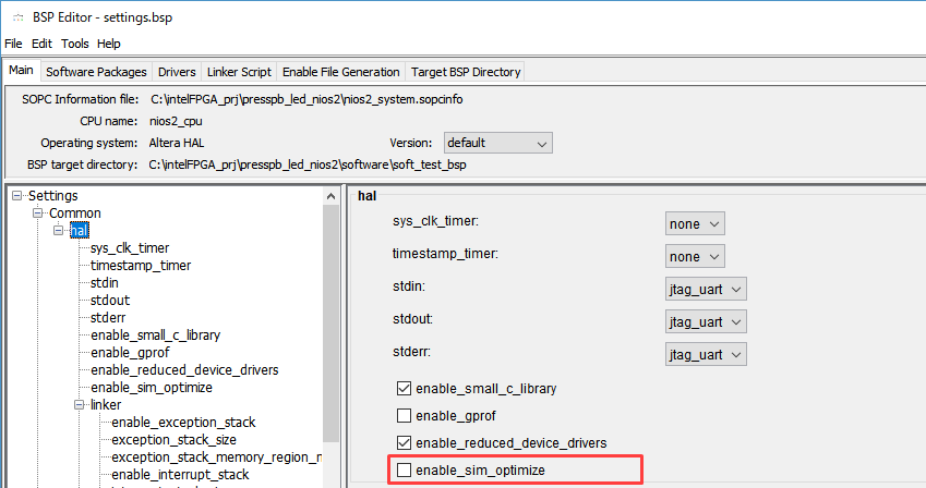
In order to turn off the option for simulation that was set at "operation 3. RTL level simulation",
Right-click on the ″software project name″_bsp folder,
Nios II➤ BSP Editor
to start the BSP Editor again and set the “enable_sim_optimize” option = Off.
[Main tab]
・Settings ➤ Common ➤ Hal
After clicking the [Generate] button and checking the log of ″INFO: Finished generating BSP files.″
Close the BSP Editor with the [Exit] button.
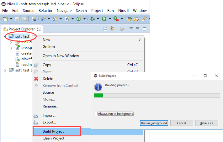
Right-click the application project (folder without _bsp) ➤ Build Project.
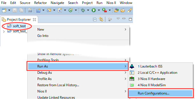
for the application project folder (the one without _bsp)
Run As➤Run Configurations
to launch the Run Configurations window.
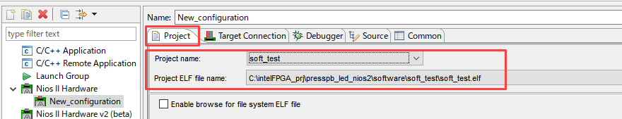
Right-click Nios II Hardware ➤ Select New.
Select the software project name in Project name in the Project tab. (soft_test in the sample project)
Select the Target Connection tab and click the [Refresh Connections] button in the upper right.
As shown in the figure, the USB-Blaster II is detected and the connection with the target board can be confirmed.
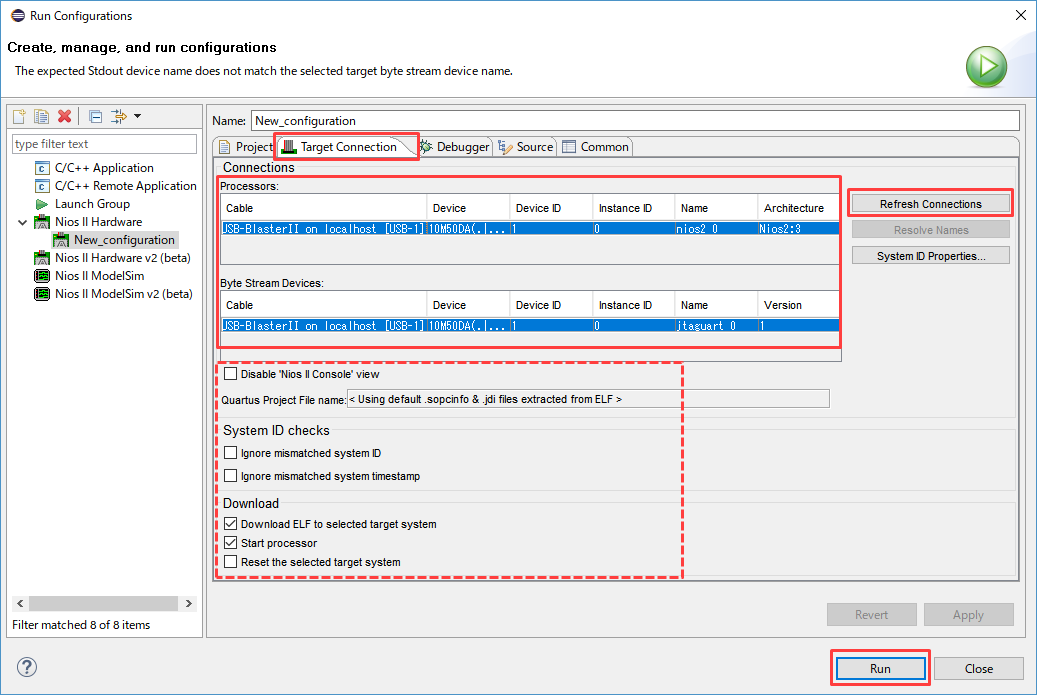
The options in the dotted frame are left as default for this sample project.
Set as necessary.
[Notes]
Details for each option are provided below.
Using the Run/Debug Configuration settings in the Nios® II SBT for Eclipse
Click the [Run] button at the bottom right of the screen.
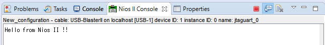
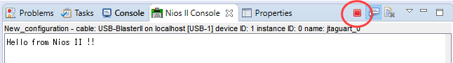
You can check the output character (Hello from Nios II !!) of the alt_printf function written on the C language source in the Console window.
You can see that the Nios ® II has executed the software program.
Now, let's actually push the push button [S1] on the MAX ® 10 FPGA development kit.
(Click the image to see the video.)
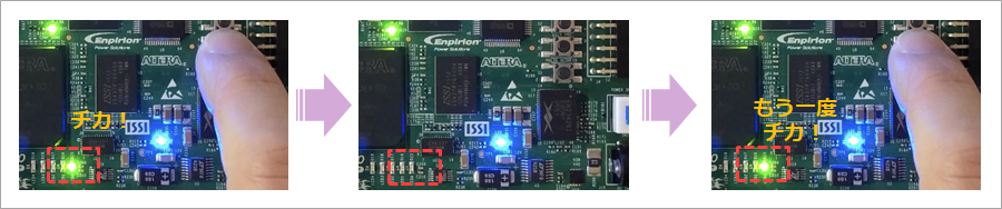
I made it!
Nios ® II is running the boot program and lighting the LEDs.
Successful Nios ® II flashing L! !
Once you're sure it works, quit the program by clicking the red button in the upper right corner of the Nios II Console window.
Since MAX® 10 is FPGA = programmable device,
If you change the output pin number to the pin number connected to another LED, the position of the LED that lights up will also change.
Also, by changing the contents of the Nios ® II boot program, you can change the operation that is executed without changing the pin assignment.
9. Embed the Nios® II boot program into the FPGA's on-chip memory
From here, a little step up from Nios ® II beginners ♪
Because the software program worked as expected on the system
Let's put this boot program into the FPGA's on-chip memory.
9-1. Convert Nios® II boot program to HEX file
In the Nios II SBT, right-click the application project (folder without _bsp) and select
Generate the HEX file of the software from the menu below.
Make Targets➤ Build...➤ mem_init_generate➤ Click the [Build]button
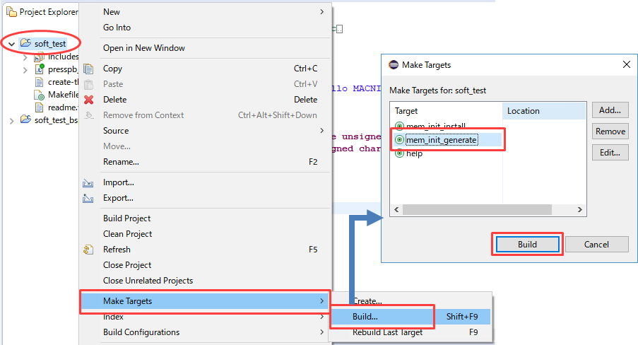
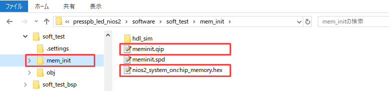
\\<application project folder>\mem_int folder
You can see meminit.qip and *_onchip_memory.hex.
9-2. Register meminit.qip in Quartus® Prime project and compile
Add meminit.qip to the project using the Quartus ® Prime menu below.
Projectmenu➤ Add/Remove Files in Project
Then compile in Quartus ® Prime.
Processingmenu➤ Start Compilation
Once compiled, you will have a .sof and a .pof containing the Nios ® II boot program.
9-3. Write to FPGA and verify actual device
Launch the Quartus ® Prime Programmer, write the .sof, and click the push button [S1] on the MAX ® 10 FPGA development kit.
Even if you don't transfer the boot program with Nios II SBT, only the sof file will blink.
Since we just wrote to the CRAM inside the MAX ® 10, the data will be erased when the board is powered off.
If you want to write programming data to CFM (Non-Volatile Flash Memory Area) in MAX ® 10
Download the .pof with Programmer.
Now even if you power off the board, the data will not be lost.
This is the end of the Nios ® II L blinking work.
Nios® II boot program quick update method
If you want to update only the Nios ® II boot program (that is, the initial value data in the on-chip memory) without changing the FPGA design
It will recompile, but there is actually a quick way to update without doing a full compile.
Note that this time-saving method can be used if meminit.qip is already registered in the Project menu ➤ Add/Remove Files in Project.
It is assumed that there is a track record of full compilation.
(Please refer to this "Without meminit.qip" for how to shorten the update time without meminit.qip.)
(1) Change the program contents with Nios II SBT and execute Build Project.
(2) Right-click the application project (folder without _bsp) and update the Hex file using the menu below.
Make Targets ➤ Build... ➤ mem_init_generate ➤ Click the [Build] button
(3) Update only the initial value data part of the on-chip memory using the following menu of Quartus ® Prime.
Processingmenu➤ Update Memory Initialization File
④ The Quartus Prime menu below generates a .sof file in which only the initial value data in the on-chip memory is updated.
Processingmenu➤ Start➤ Start Assembler
Please use this .sof to create pof and jic.
Nios® II boot program quick update method (without meminit.qip)
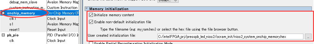
This time-saving method uses specific on-chip memory initialization settings created in Platform Designer.
It is assumed that there is a track record of full compilation.
(1) Change the program contents with Nios II SBT and execute Build Project.
(2) Right-click the application project (folder without _bsp) and update the Hex file using the menu below.
Make Targets➤ Build...➤ mem_init_generate➤ Click the [Build] button
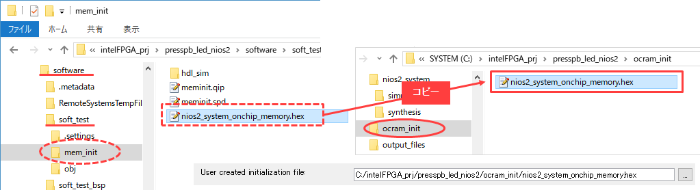
(3) Overwrite and copy the *_onchip_memory.hex file generated in (2) to the initial value file specified in the on-chip memory.
(4) Update only the initial value data part of the on-chip memory using the following menu of Quartus ® Prime.
Processingmenu➤ Update Memory Initialization File
⑤ The Quartus ® Prime menu below generates a .sof file in which only the initial value data in the on-chip memory is updated.
Processingmenu➤ Start➤ Start Assembler
Please use this .sof to create pof and jic.
The sample design this time was an easy-to-understand, simple circuit that just connects pins.
Expanding it further to create logic circuits and Nios ® II systems opens up a wide range of possibilities.
Everyone please try it.
■ Sample project
The design of L Chika this time can be created from scratch as per this content
If you want to start using the actual machine immediately, please usethe sample project in which operations 1 to 8 have been performed.
* This sample project was created with Quartus ® Prime Standard Edition 20.1.0 Build711.
* When using the software project of the sample project,
Please execute Generate BSP and Build Project in your own environment before using.
Also, when executing Run Configuration, enable the following options and execute Run.
・Ignore mismatched system ID = On
・Ignore mismatched system timestamp = On
Click here for recommended articles/materials
Getting started with Intel® FPGA
The first L blinking with Intel® FPGA!
The first LED blinking on Intel® FPGA Nios® II! Part 1
The first LED blinking on Intel® FPGA Nios® II! Part 2
Boot Nios® II with FPGA's on-chip memory
Boot Nios® II with UFM in MAX® 10
Nios® II Processor on Intel® FPGA
Click here for recommended seminars/workshops
"Nios® II Introductory Edition Trial" released in video!
"Custom Microcomputer Design Trial" released in video!
Intel® Cyclone® 10 LP FPGA Seminar In a Box