- Semiconductor BusinessHOME
- Products and Services of Macnica,Inc.
-
technical information

-
Events and Seminars
- Handling Manufacturer
- Support
- Inquiry
- Click here to purchase products
- Semiconductor business e-mail magazine registration
![]()
![]() Narrow down by specifying conditions
Narrow down by specifying conditions
現在2183件がヒットしています。check


hello.
My name is Intel F. Hanako and I provide technical support for Intel® FPGA products at Macnica.
There are two ways to embed the Nios® II boot program into the on-chip memory inside the MAX® 10 FPGA.
- Embedded in on-chip flash
- Embedded in on-chip RAM
Reference: Booting Nios® II on FPGA's on-chip memory
This time, we will show you how to embed a Nios® II boot program into the User Flash Memory (UFM), the on-chip flash of MAX® 10.
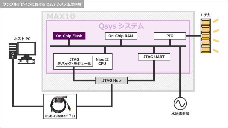
Overview of this design
The Qsys system I created this time is
The boot program memory is on-chip flash (UFM), and the executable program memory is on-chip RAM.
This is an extremely simple design that blinks an LED when Nios ® II boots.
About UFM capacity
The MAX ® 10 has a non-volatile flash memory area (UFM/CFM).
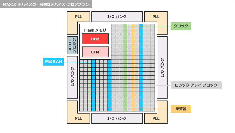
The UFM capacity is shown in the table below.
| Device | 10M02 | 10M04 | 10M08 | 10M16 | 10M25 | 10M40 | 10M50 |
| Total User Flash Memory Size (Kb) (*) | 96 | 1,248 | 1,376 | 2,368 | 3,200 | 5,888 | 5,888 |
(*) This is the maximum value that can be specified, depending on the selected mode.
If the Nios ® II boot program fits within this size, you can specify the UFM as the boot memory.
To check the size of the boot program, refer to the program size of the elf file displayed on the Console screen when building it with the Nios® II Software Build Tool (hereinafter referred to as Nios® II SBT).
For more information about UFM, see the following document:
MAX 10 User Flash Memory User Guide (PDF)
Operation flow
It is assumed that Nios ® II and peripherals other than On-Chip Flash have already been configured in Qsys.
1. Add On-Chip Flash to your Qsys system
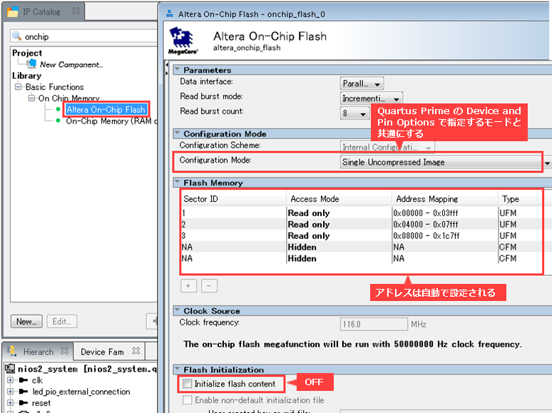
To use the MAX ® 10 UFM, you need to incorporate a free IP called “Altera On-Chip Flash”.
Launch Qsys from the Tools menu and double-click “Altera On-Chip Flash” from the IP Catalog (top left of the screen).
- Select the Configuration Mode.
There are three configuration modes that support UFM boot. Select the mode according to your system specifications.
Single Uncompressed Image
Single Compressed Image
Dual Compressed Images
In this design, the program is very small and the UFM is not used for anything other than boot memory, so we selected Single Uncompressed Image.
・ Flash Memorydetermines the sector configuration of the on-chip memory.
Select the access mode for each sector from Read only / Read and write / Hidden.
In this design, the UFM is used only as Nios® II boot memory, so it is set to read only.
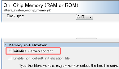
- Turn off the Initialize flash content option.
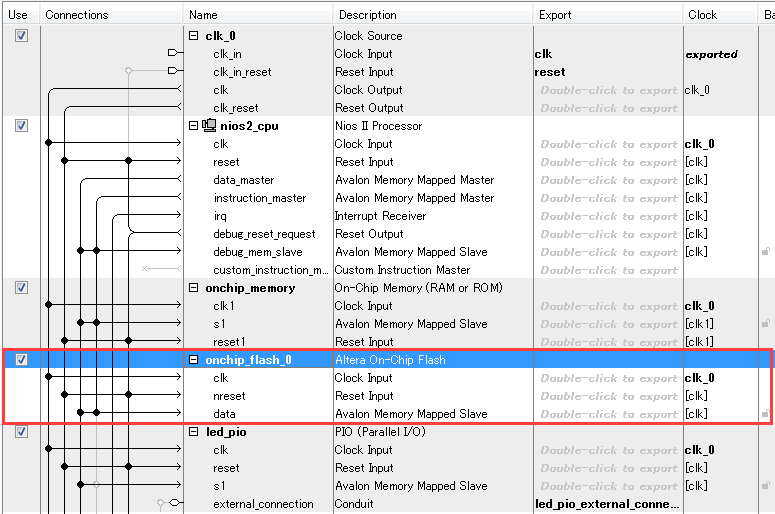
Connect the On-Chip Flash to the Qsys system.
A little point of Hanako♪
None of the three Configuration Modes that can be selected for On-Chip Flash support memory initial values, so the on-chip memory (RAM) built into the Qsys system cannot retain the initial values.
Therefore, set the Initialize memory content option = OFF.
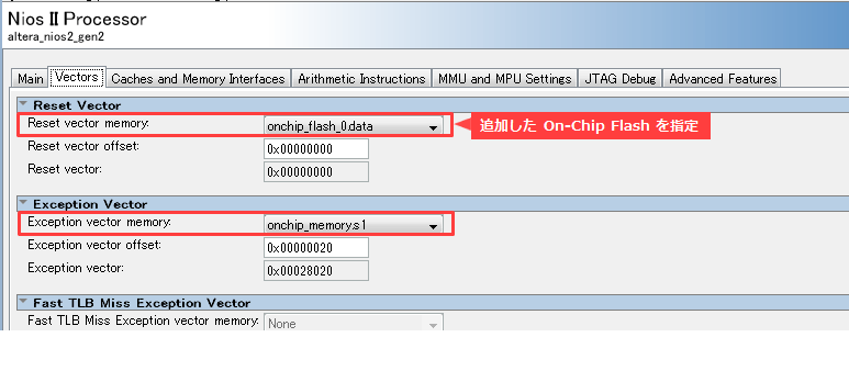
2. Specifying Boot Memory for Nios® II
Specify the Nios ® II Vectors tab as follows:
3. Run Generate HDL to generate the Qsys system module
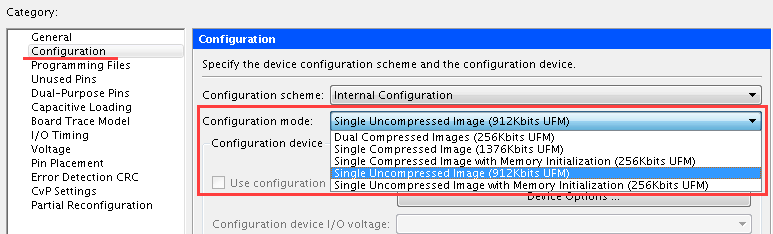
4. Change Configuration Mode in Quartus® Prime
Select the same Configuration Mode that you selected for the On-Chip Flash built into Qsys.
Assignments menu > Device > Device and Pin Options > Configuration
5. Compile in Quartus® Prime (Start Compilation)
This is the end of the first part.
Read more in this technical article.
Booting Nios® II with MAX® 10 UFM [Part 2]
In the second part, we will perform the following operations.
- Set up BSP Editor on Nios® II SBT and run Generate
- Convert boot program to HEX file with Nios® II SBT
- Conversion of programming files
- Programming to MAX® 10
Related article
Boot Nios® II with FPGA's on-chip memory
Let's boot Nios® II with MAX® 10 UFM [Part 2]
Related FAQ
Can MAX® 10 Compact devices set initial values to M9K memories?
Can Nios® II run only on the on-chip memory of an FPGA?
Related products
Odyssey MAX® 10 FPGA EVA Kit
MAX® 10 FPGA Development Kit
Nios® II Embedded Evaluation Kit with MAX® 10