- 半導体事業HOME
- マクニカの製品・サービス
-
技術情報

-
イベント・セミナー
- 取扱メーカー
- サポート
- お問い合わせ
- 製品購入はこちら
- 半導体事業のメルマガ登録
![]()
![]() 条件を指定して絞り込む
条件を指定して絞り込む
現在2004件がヒットしています。check


こんにちは。
マクニカでインテル® FPGA の技術サポートをしている インテル・F・ハナコ です。

■ 用意するもの
Quartus® Prime Standard Edition
または Lite Edition (無償)
ModelSim* - Intel® FPGA Edition
または
ModelSim - Intel FPGA Starter Edition (無償)

■ 開発ボードの接続構成
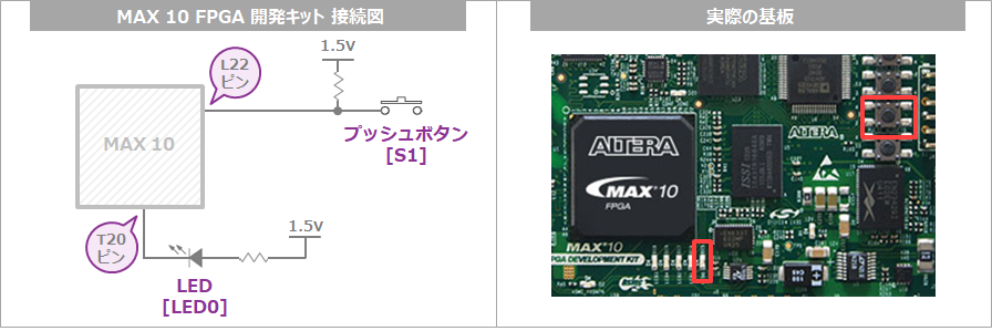
プッシュボタン [S1] と LED [LED0] は、基板上で図のような接続構成になっています。
プッシュボタンを押したら LED が点灯して、プッシュボタンを離すと LED も消灯する
この説明だけだと「なんだ、線でつなぐだけじゃん!」って思いますよね。
そうなんです!
プッシュボタンが接続している FPGA のピンと、LED につながっている FPGA のピンを、単純につなげばいいんです。
でも、つなぐって…どうやって…?
FPGA のは中身が空っぽのただの箱です。(※ あくまでもイメージです。)
なので、プッシュボタンからの入力信号を FPGA が受信して、FPGA を通り、
その信号を LED へ出力するための ″デジタル論理回路″ を設計しましょう。
■ Quartus Prime で設計スタート!
インテル FPGA の開発ソフトウェア Quartus Prime を使用し、
インテル FPGA の開発フロー/トップページ で紹介されているフローに基づいて作業を進めます。
(各作業へのショートカットは、画面左側の項目をクリックしてご利用ください。)
1. 論理回路を設計する
1-1.
プロジェクトを作成 します。
File ➤ New Project Wizard
ここでは、プロジェクト名と最上位エンティティ名を presspb_led に設定します。
ターゲットデバイスは、MAX 10 ファミリーの 10M50DAF484C6GES を選択します。
1-2.
Quartus Prime の下記メニューから、VHDL または Verilog HDL 用のワーキングシートを開き、
HDL 言語で論理回路 (以下 デザイン) を書きます。
File ➤ New ➤ Design File カテゴリ ➤ VHDL File または Verilog HDL File
サンプルはこんな感じ。
-- VHDL sample : presspb_led.vhd


library ieee;
use ieee.std_logic_1164.all;


entity presspb_led is
	port (
		PB	 :  in  std_logic;
		LED 	 :  out std_logic
	     );
end;


architecture rtl of presspb_led is
begin
	LED <= PB;
end rtl;
// Verilog HDL sample : presspb_led.v
module presspb_led
(
input PB,
output LED
);
assign LED = PB;
endmodule
1-3.
Quartus Prime の下記メニューにより、デザインファイルを保存します。
ここでは、ファイル名を presspb_led.vhd、presspb_led.v とします。
File ➤ Save As
1-4.
Quartus Prime の下記メニューを実行して記述ミスが無いかをチェックし、データーベースを構築します。
Processing ➤ Start ➤ Start Analysis & Elaboration
2. 論理シミュレーションをする
ModelSim - Intel FPGA Edition または ModelSim - Intel FPGA Starter Edition で
自分が作成したデザインの RTL レベル・シミュレーションを行います。
・実行するための環境設定や基本作業フローは、こちらのコンテンツ を参考にしてください。
・今回のデザイン用のテストベンチ・ファイルは、以下よりダウンロードしてください。
プロジェクトフォルダーへ保存し、ファイル名を testbench.vhd / testbench.v に変更してください。
2-1.
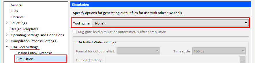
Quartus Prime の下記メニューより、NativeLink シミュレーションのセットアップをします。
Assignments ➤ Settings ➤ EDA Tool Settings ➤ Simulation
ここでは 以下のとおりに設定します。
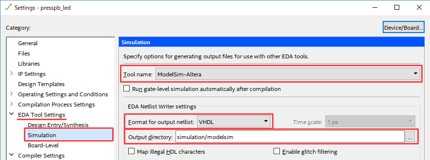
|
Tool name |
ModelSim-Altera (ModelSim - Intel FPGA Edition のこと。Starter Edition もこれを選択) |
|
Format for output netlist |
設計に選択した言語 |
|
Output directory |
simulation/modelsim (デフォルトのまま) |
2-2.
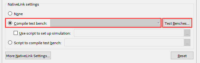
NativeLink settings 内から Compile test bench を選択し、Test Benches ボタンをクリックします。
Test Benches ウィンドウの New ボタンをクリックし、New Test Benches Settings ダイアログボックスを設定します。
ここでは以下のとおりに設定します。
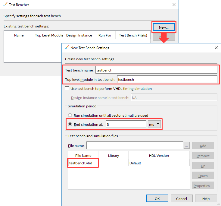
|
Test bench name および Top level module in test Bench |
testbench |
|
Simulation period |
End simulation at を選択 / 3 ms に設定 |
|
File name |
ブラウズボタをクリックし、ダウンロードしたテストベンチ・ファイルを選択。Add ボタンで登録 |
各ウィンドウを OK で閉じます。
2-3.
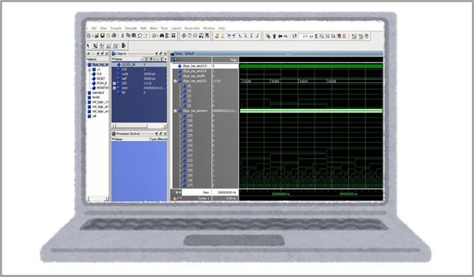
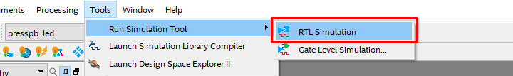
Quartus Prime の下記メニューから、NativeLink でファンクション・シミュレーションを実行します。
Tools メニュー ➤ Run Simulation Tool ➤ RTL Simulation
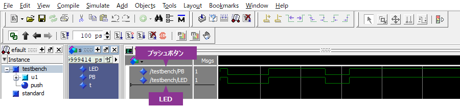
ModelSim - Intel FPGA Edition のオペレーションが自動的に実施され、Wave ウィンドウに波形が表示されます。
この波形が、期待動作かを確認します。
2-4.
ModelSim - Intel FPGA Editionのメニューから Simulate ➤ End Simulation を選択し、シミュレーションを終了します。
続いて File ➤ Quit を選択し、ModelSim - Intel FPGA Edition のGUI を閉じます。
2-5. (任意作業です。)
Quartus Prime の下記メニューを None に戻します。
Assignments ➤ Settings ➤ EDA Tool Settings ➤ Simulation
3. 制約を設定する
作業は Quartus Prime に戻ります。
3-1.
ピン番号を指定 します。
デザイン上の入力ピン (PB) と出力ピン (LED) を、MAX 10 の目的のピン番号に割り当て、I/O 規格を設定します。
Pin Planner では、Location (ピン番号) と I/O Standard (I/O 規格) をこのように設定します。
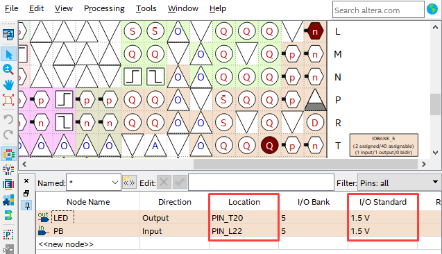
各ピンの I/O Standard を "1.5 V" にしている理由は
MAX 10 FPGA 開発キット上の MAX 10 のピン T20、L22 が I/O Bank 5 に属していて
その I/O バンク(※) の電源は 1.5 V が供給されているからです。
だから LED のプルアップ電源も 1.5 V なんです。
[参考情報] I/O バンクとは?
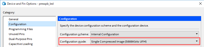
3-2.
コンフィグレーション・モードを選択 します。
MAX 10 の CFM (コンフィグレーション用フラッシュメモリ) をどう使うか = 何モードを選ぶか、になるのですが
今回は "Single Compressed Image" を選択します。
Assignments ➤ Device ➤ Device and Options ➤ Configuration ➤ Configuration mode
3-3.
デザインに対する タイミング制約を作成&設定 します。
今回はクロック制御とは無関係で、スピードを必要とする論理回路ではないですし
Pin to Pin の超単純動作なので省略します。
4. コンパイルをする
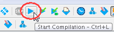
いよいよでデザインをコンパイルします。
Processing ➤ Start Compilation
論理合成と配置配線が実行され、FPGA 内部に書き込むプログラムデータも同時に生成されます。
5. タイミング検証をする
コンパイル終了後に、生成された コンパイル・レポートを検証 します。
なお、この L チカでは省略しますが
通常の開発では、Timing Analyzer レポートの内容を確認し、タイミング制約で与えた条件を満たす結果になったか タイミング検証 します。
タイミング違反している場合には、Timing Analyzer を使用し詳細な解析を行いながら改善に努めます。
6. プログラミングをする
Quartus Prime の下記メニューから Programmer を起動し、基板上の MAX 10 にデータを転送します。
Tools ➤ Programmer
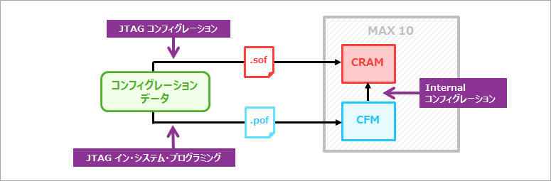
MAX 10 をコンパイルすると、2種類の書き込み用ファイル (.sof / .pof) が生成されます。
今回は実機で動作確認をする目的 (つまり デバッグ) でデータを転送したいので
MAX 10 内の CRAM(Configuration RAM)に SOF ファイルをダウンロードします。
MAX 10 FPGA 開発キットとパソコンを mini-USB ケーブルで接続します。
電源ケーブルを接続し、ボードに電源を供給 (On) します。
[参考情報] USB-Blaster II ドライバーのインストール
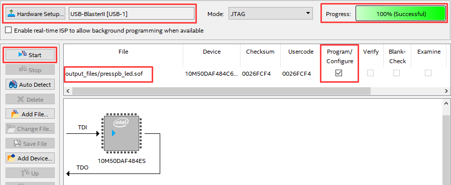
Programmer において、Hardware Setup から USB-Blaster II を選択し
presspb_led.sof をセット後、Start ボタンをポチッ♪
Programmer の Progress バーが 100% になったら、データ転送完了です。
■ いざ!実機で動作検証
MAX 10 FPGA 開発キット上のプッシュボタン [S1] を ポチッ♪と押してみましょう。
(画像をクリックすると、動画が見られます。)

おぉ、Lチカ!できました!
今書き込んだのは MAX 10 内の CRAM なので、ボードの電源を OFF にするとデータは消去されます。
デバッグが終了したら、プログラミング・データを MAX 10 内の CFM (不揮発性の Flash メモリ領域) に書き込むために
Programmer で presspb_led.pof をダウンロードしてください。
これでボードの電源を OFF っても、データは消えることはありません。
MAX 10 は FPGA = プログラマブル・デバイスですから
今回の論理回路はそのままに、出力ピンの番号を別の LED に接続されているピン番号に変更すれば
点灯する LED の位置も変わります。是非お試しあれ!
今回は わかりやすくピンとピンをつなぐだけのシンプルな回路でしたが
もっともっと拡張して論理回路を作れば、様々な可能が広がります。
みなさんも是非挑戦してみてください。
インテル FPGA で はじめての L チカ [第2弾] は、FPGA に Nios® II を入れてLチカ したいと思います。
お楽しみに!
■ サンプルプロジェクト
今回の L チカのデザインは、このコンテンツどおり ゼロ から作成できますが
すぐに実機動作させたい場合は、以下のサンプルプロジェクトをご利用ください。
※ QAR ファイルの展開方法は、「Quartus Prime - プロジェクトの管理」の ″アーカイブ・プロジェクトの復元″ をご覧ください。
※ プロジェクトの復元方法は、「Quartus Prime はじめてガイド - プロジェクトの作成方法」の ″既存プロジェクトの起動方法″ をご覧ください。
今回の Quartus Prime での一連の作業は、こちらの動画でもご覧いただけます。
おすすめ記事/資料はこちら
はじめての インテル FPGA 設計 [デモ動画]
FPGA に Nios® II を入れてLチカ!Part 1