- Semiconductor BusinessHOME
- Products and Services of Macnica,Inc.
-
technical information

-
Events and Seminars
- Handling Manufacturer
- Support
- Inquiry
- Click here to purchase products
- Semiconductor business e-mail magazine registration
![]()
![]() Narrow down by specifying conditions
Narrow down by specifying conditions
現在2004件がヒットしています。check

Hello. My name is Taro Washimiya and I provide technical support for Intel® FPGA products at Macnica.
We provided an overview of FPGA PLLs in "Intel® FPGA PLLs," but here we will explain the steps to use the PLL Intel FPGA IP.
To see which FPGA families can use the PLL Intel FPGA IP, see PLLs in Intel® FPGAs.
content
tools to use
- Intel® Quartus® Prime Standard Edition Development Software
- ModelSim® - Intel® FPGA Edition
See the Quartus® Prime Edition Comparison for the relationship between target FPGAs and development tool editions.
If you don't have the development software installed, you can get it from the Intel® FPGA website.
For details, please see the content below.
How to Download Intel® Quartus® Prime Software and ModelSim® - Intel® FPGA Edition
How to Install Intel® Quartus® Prime Software and ModelSim® - Intel® FPGA Edition
1. Generating PLL IP
Here, Cyclone® V project is used as an example.
Open a project whose target device is Cyclone® V, or create a new project.
(For Quartus® Prime project creation, refer to Quartus® Getting Started Guide - How to Create a Project.)
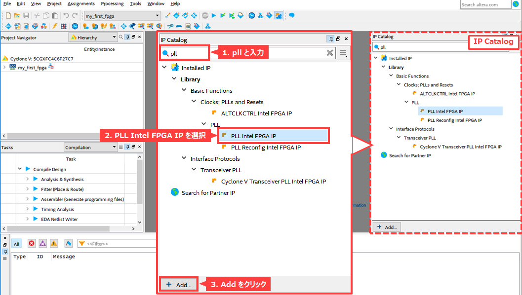
Type pll into the IP Catalog search bar within Quartus® Prime.
Then you can easily locate the PLL Intel FPGA IP.
With PLL Intel FPGA IP highlighted, click Add.
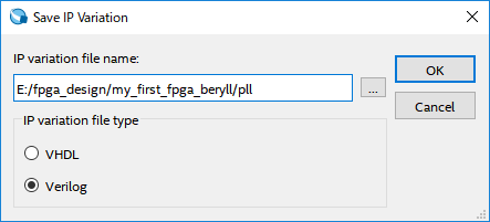
Specify the folder path to generate the PLL Intel FPGA IP, the name you want to give to the PLL Intel FPGA IP, the language to generate (VHDL or Verilog), and click OK.
It is recommended to generate in the working folder of the project or its lower folder.
The PLL Intel FPGA IP Settings window launches.
Here, if you want to see detailed documentation and explanations of each setting item, click Documentation.
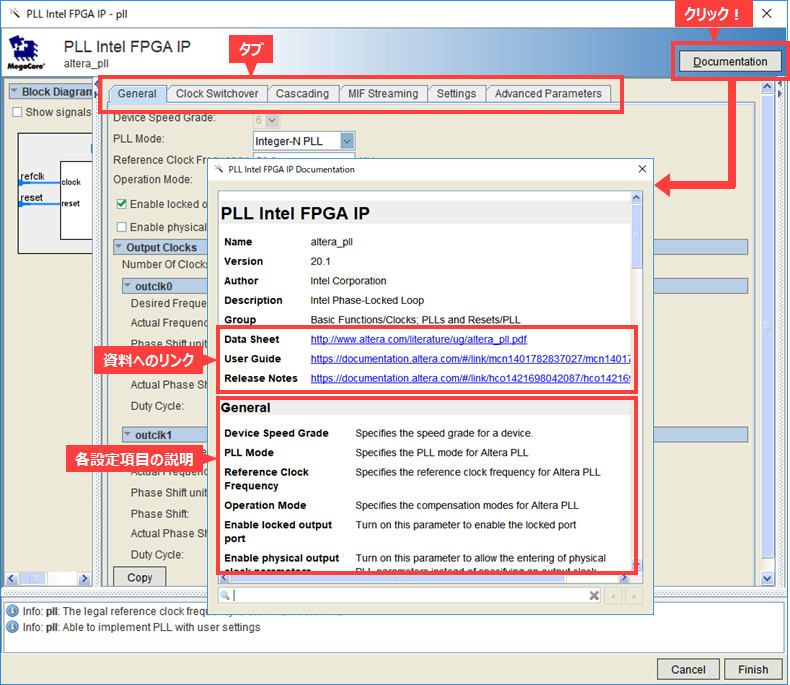
This section briefly describes the main setting items in each tab.
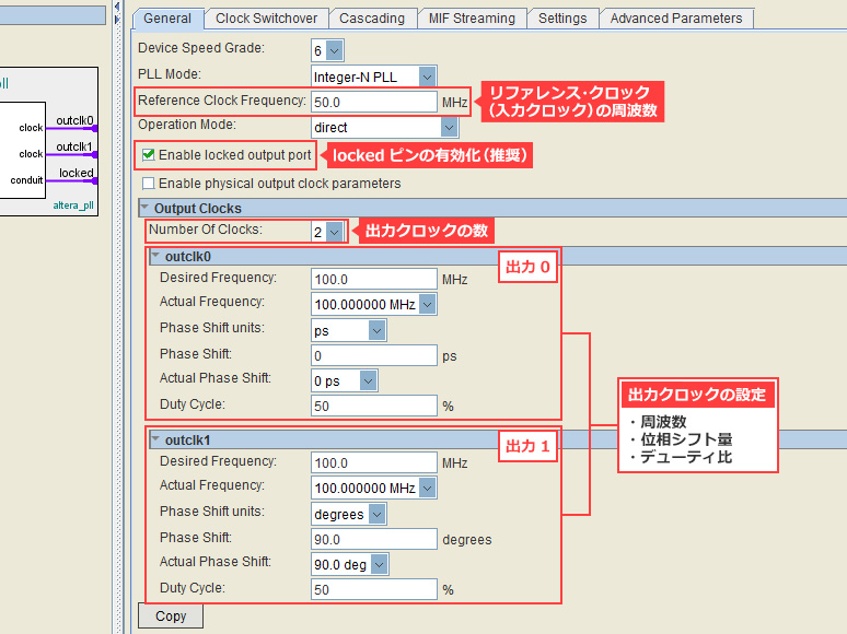
General tab
Configure general settings such as reference clock (input clock) frequency, locked pin enable/disable, number of output clocks, and output clock settings.
Here, as an example, we will configure the settings as shown in the table below.
|
Item |
set value |
|
Reference clock frequency (input clock frequency) |
50 (MHz) |
| Operation Mode | direct |
| Enable locked output port | On |
| Number Of Clocks | 2 |
| outclk0 (output 0) | |
|
Desired frequency (output clock frequency) |
100 (MHz) |
|
Phase shift (phase shift value) |
0 (ps) |
| Duty cycle | 50 (%) |
| outclk1 (output 1) | |
|
Desired frequency (output clock frequency) |
100 (MHz) |
|
Phase shift (phase shift value) |
90 (degrees) |
| Duty cycle | 50 (%) |
The following tabs are briefly described. For details on each item, see the user guide from the link to the document introduced earlier.
Clock Switchover tab
Depending on the FPGA series, it supports a function to switch with 2 inputs, and it is set.
Cascading tab
Depending on the FPGA series, PLL cascade connection is supported, and this setting is made.
MIF Streaming tab
Set the Dynamic Phase Shift function using the MIF file that stores the PLL setting data.
Cyclone® V does not support this feature.
Settings tab
Configure settings for PLL auto-reset, PLL bandwidth preset, dynamic reconfiguration, dynamic phase shift, and dynamic phase alignment (DPA).
Advanced Parameters Tab
You can see the PLL parameter names and values, such as the PLL M/N/C counter values and VCO frequency.
After finishing various settings, click Finish to generate the IP.
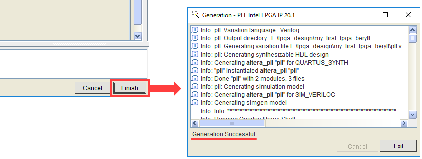
After confirming "Generation Successful" and clicking Exit, the following window will appear.
Click Yes to add the generated IP design to the currently open project. (If you click No, please add it manually.)
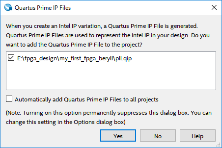
You have now completed generating the PLL Intel FPGA IP.
Let's proceed with logic design by connecting with the user circuit you are designing.
If you want to change the settings of the PLL Intel FPGA IP, please refer to this FAQ.
[FAQ] How to start IP editing screen
After editing the required parameters, generate the PLL Intel FPGA IP again.
2. Connection with user circuit
After the PLL Intel FPGA IP is generated, connect it with user logic.
If you are not familiar with Verilog-HDL or VHDL, please refer here. See Calling Subordinate Modules (Blocks) within this page.
Let's start! Verilog-HDL <with exercises>
Let's start! VHDL <with exercises>
If you are designing with a schematic (circuit diagram), a symbol for the schematic editor is also generated when the IP is generated, so please call and connect the IP symbol created by the user on the schematic editor.
However, the schematic cannot be RTL simulated in 3rd party tool simulators. Again, it is recommended to design in HDL.
<Tricks>
If you are not familiar with writing HDL, try using the schematic-to-HLD conversion feature in Quartus® Prime's schematic editor.
Please refer to the document on the following page for how to convert.
Getting Started with Quartus® - Using the Schematic Editor
After creating the design files for the upper hierarchy,
Select Processing > Start > Start Analysis & Synthesis from the Quartus® Prime menu to perform logic synthesis.
Did it complete successfully?
When converting from a schematic, if both the schematic file (BDF file) and the converted HDL file (V file for Verilog-HDL, VHD file for VHDL) are registered in the project, logic synthesis cannot be performed correctly. . (Remove unused design files from Project menu > Add/Remove Files in Project.)
3. Check by simulation
Now let's check it in RTL simulation.
This time we will use ModelSim® - Intel® FPGA Edition.
A testbench is required for verification in simulation, but the testbench is created by the user.
See here for how to write a testbench.
Let's start! Test bench
Once you have your testbench, you are ready to simulate.
You can manually navigate ModelSim® to run the simulation, but here are some useful methods. please refer.
Simulation using NativeLink functionality
Let NativeLink solve your FPGA function simulation
Let's generate and run a simulation script file for ModelSim®
Simulating with msel_setup.tcl
How to edit and use msim_setup.tcl
So far, Taro Washinomiya introduced the steps from creation of PLL Intel FPGA IP to simulation.
Click here for recommended articles/materials
PLL division/multiplication
Application of PLL (Let's reduce EMI with spread spectrum!)
The intimate relationship between PLL loop bandwidth and spread spectrum
PLLs in Intel® FPGAs
List of IP-related articles and materials
Intel FPGA Development Flow / Top Page