- Semiconductor BusinessHOME
- Products and Services of Macnica,Inc.
-
technical information

-
Events and Seminars
- Handling Manufacturer
- Support
- Inquiry
- Click here to purchase products
- Semiconductor business e-mail magazine registration
![]()
![]() Narrow down by specifying conditions
Narrow down by specifying conditions
現在2154件がヒットしています。check

デザインの論理検証の重要性とテストベンチ

As you all know, hardware description languages (HDL) such as Verilog-HDL and VHDL are the mainstream for FPGA development (logic circuit) design.
Before compiling and debugging on the actual machine, verification work is required to confirm that the design designed in HDL operates correctly. A logical verification of a design involves performing a simulation, but in order to perform a simulation, a "test bench" that describes the input conditions (test conditions) to the design is required separately from the design. And the testbench will be described mainly in HDL by the designer as well as the design.
Before creating a testbench, you need to think about what you want to verify and know how the design under test should behave. Please understand them properly before creating a testbench.
Here, we will focus on the minimum content that is likely to be necessary for creating a testbench that even beginners can understand, and we will explain it with description examples.
For your reference, you can download the training data from the following page.
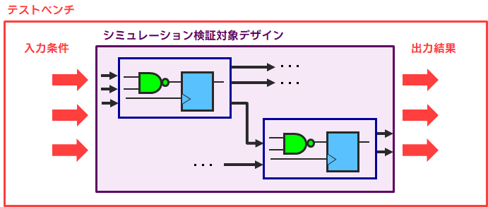
Relationship between testbench and design (circuit)
Hierarchical design techniques are mainly used to create designs (logic circuits) in FPGAs. Hierarchically speaking, the testbench resides at a higher level of hierarchy than the design under test (typically at the top level) of the FPGA design. Within the testbench, the input conditions (such as clock inputs, reset inputs, and other inputs) to the design under test are described in HDL and input to the design under test in the FPGA design located in the lower hierarchy. The input signal passes through the created design, the result is output, and by checking the result with the simulator, it is possible to judge whether the created design operates correctly.
From here on, I will explain how to write a concrete testbench in both Verilog-HDL and VHDL.
Note that the testbench module name and entity name are arbitrary. I often see cases where_tb or_sim is added to the end of the verification target design name, but this is by no means a rule. Feel free to choose a name for yourself.
Coffee break: simulator

To simulate your design, you need a simulator. For Altera FPGA users, we recommend ModelSim-Altera Edition. For information on how to use the ModelSim-Altera Edition, please see our published documentation.
Coffee Break: Leveraging NativeLink Features
Altera's FPGA/CPLD development tool Quartus Prime/QuartusII development software can automatically run the EDA simulator from Quartus Prime/Quartus II to display the simulation results.
This NativeLink feature saves you the trouble of manually launching the simulator, compiling, loading the design, and so on. But don't forget that you'll need to create a testbench beforehand...
Let NativeLink solve your FPGA function simulation
Quartus Getting Started Guide – How to set up EDA tools
* EDA: A general term for software, hardware, and methods for automating and supporting electronic design work such as electronic devices and semiconductors.