- Semiconductor BusinessHOME
- Products and Services of Macnica,Inc.
-
technical information

-
Events and Seminars
- Handling Manufacturer
- Support
- Inquiry
- Click here to purchase products
- Semiconductor business e-mail magazine registration
![]()
![]() Narrow down by specifying conditions
Narrow down by specifying conditions
現在2164件がヒットしています。check

In this column, most of the time, signals transmitted through distributed constant circuits are treated as pulse responses, that is, transient phenomena.
Not only for distributed constant circuits, but also for circuits in general, there are two types of signal responses: time response and frequency response.
Both can be exchanged by Fourier transform.
This time, let's look at the distributed constant circuit on the frequency axis. I will divide it into two parts.
See also
Laplace transform and Fourier transform
It is convenient to use tandem sequences to find the response of a distributed parameter circuit.
See below for vertical columns.
vertical row
Longitudinal sequence and waveform analysis of distributed constant line
vertical row
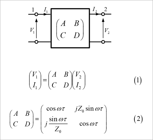
Figure 1 is the vertical sequence mentioned in the column above.
As shown in equation (1) in the figure, the input voltage and current are represented by the output voltage and current. Therefore, it is suitable for expressing the behavior of cascade connections. Equation (2) expresses each component in the tandem of the line as a function of the angular frequency ω and the propagation delay time τ of the line.
Near/far end voltage/current
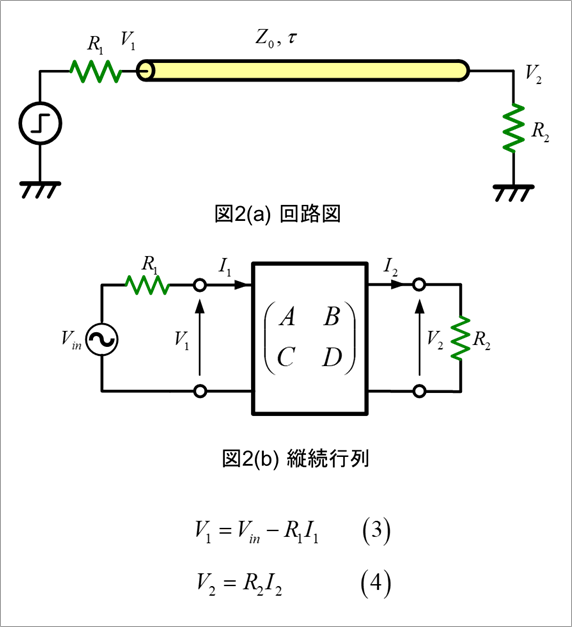
Figure 2(a) is a circuit diagram of lines and input/output resistors. The near end resistance is R1, the far end resistance is R2, the line is characteristic impedance Z0, and the one-way propagation delay time is τ. Figure 2(b) is the schematic rewritten in vertical columns.
Equations (3) and (4) show the relationship between voltage V1 and current I1 on the input side and voltage V2 and I2 on the output side.
Equation (5) is obtained by substituting equations (3) and (4) into equation (1).
Equations (6) and (7) are the simultaneous equations with V1 and V2 as unknowns by rearranging Equation (5).
Equation (8) is a rewrite of Equations (6) and (7).
Solving equation (8) for V1 and V2 yields equations (9) and (10).
By substituting equation (2) for these, we obtain the frequency characteristics of V1 and V2.
By actually transforming and arranging the equations, it is possible to obtain conditions such as no waveform distortion for near-end waveform V1 and far-end waveform V2. If you are interested, please see the references.
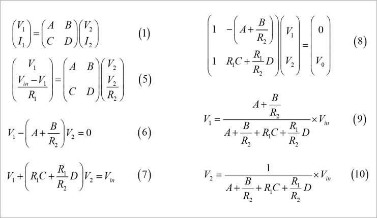
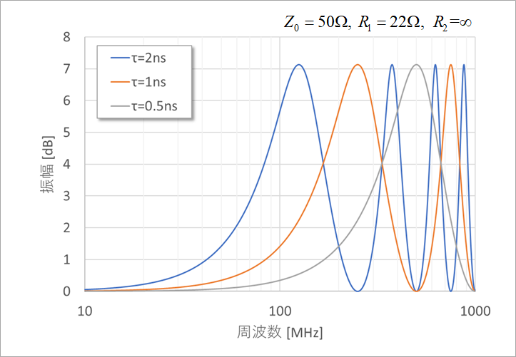
Figure 4 shows the frequency characteristics of V2/Vin in equation (10) with R1 as a parameter. It's the output voltage with respect to the input voltage, so it's a transfer function. As R1 becomes smaller, the peak value of frequency characteristics becomes larger. A small R1 indicates a large drive capability of the driver. R1=11Ω corresponds to a drive capacity of about 24mA, 22Ω to 12mA, and 33Ω to 8mA. The peak frequency is approximately 250MHz. This frequency is described below.
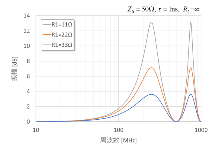
Figure 5 shows the time response of V2 when a square wave is applied to the input of Figure 2(a). Comparing Figures 4 and 5, we can see that the frequency and time responses vaguely correspond. The pulse width of this reflected waveform is 2ns. Since the one-way time of the railroad track is 1 ns, it is one round trip. Applying a sine wave to this waveform gives a period of 4 ns and a frequency of 250 MHz. The inverse fast Fourier transform (iFFT) is used to obtain the time response from the frequency response.
See below.
FFT by Excel
FFT by Excel (Part 2)
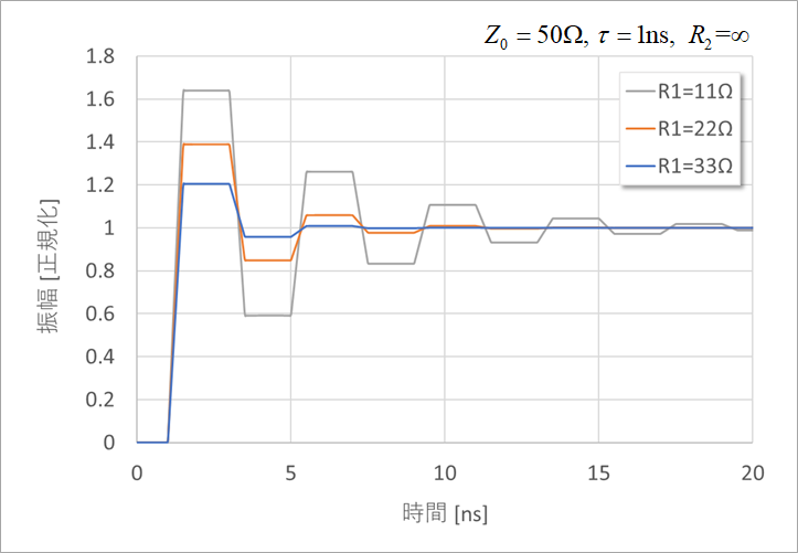
Figure 6 shows the frequency response for different wire lengths. τ=1ns is approximately 15cm.
The frequency of the peak is 1/(4τ).
Equation (11) in Figure 7 shows the transfer function for normal CMOS transmission with R2 = ∞ in Equation (10), ie, open-ended at the far end. Equation (12) is its absolute value. In the case of normal CMOS transmission, R1<Z0. Therefore, as shown in Equation (13), when cosωτ=0, the maximum value is Z0/R1, which is shown in Equation (14). , the minimum value is 1 (0 dB) when cosωτ=±1.
Equation (15) is the frequency at which the peak is taken.
Since ω=2πf, the first peak is 1/(4τ).
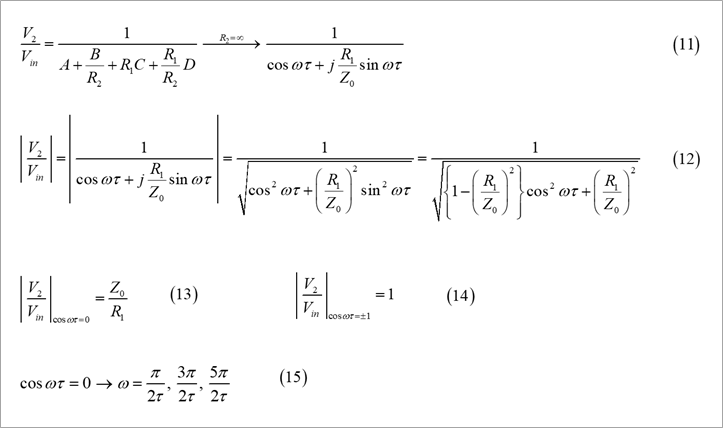
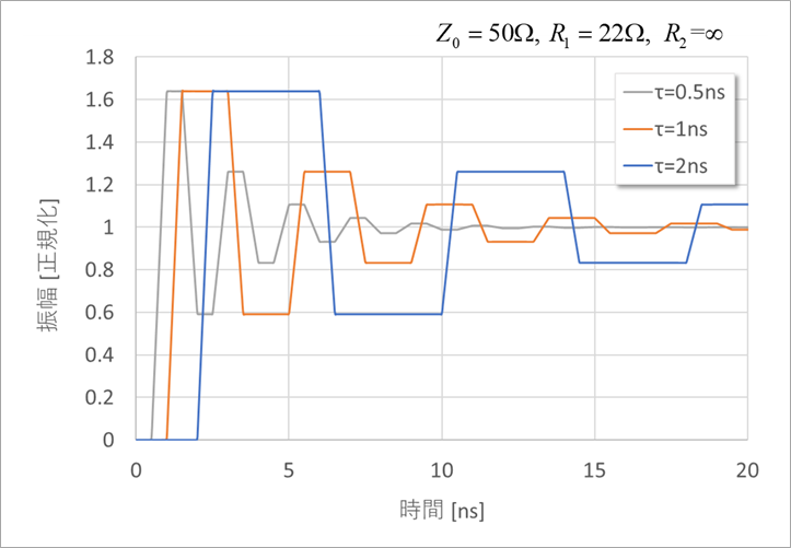
Figure 8 shows the time response when the line length in Figure 6 is varied. The period of oscillation of the reflected wave matches the peak of the frequency characteristic. For example, when τ=2ns, the peak in Figure 6 is 1/8ns=125MHz and the oscillation period is 8ns. When τ=0.5ns, 1/2ns=500MHz, period is 2ns.
In this way, there is a certain relationship between the frequency response and the time response, and the absolute value of the frequency response is calculated directly in Excel, and the common logarithm is multiplied by 20 to obtain decibels. The time response can be easily obtained with the inverse fast Fourier transform (iFFT).
References
Yuzo Usui: All About Distributed Constant Circuits for Board Designers (3rd Edition) Self-published, pp.146-169, 2016
What is Yuzo Usui's Specialist Column?
It is a series of columns that start from the basics, include themes that you can't hear anymore, themes for beginners, and also a slightly advanced level, all will be described in as easy-to-understand terms as possible.
Maybe there are other themes that interest you!