- Semiconductor BusinessHOME
- Products and Services of Macnica,Inc.
-
technical information

-
Events and Seminars
- Handling Manufacturer
- Support
- Inquiry
- Click here to purchase products
- Semiconductor business e-mail magazine registration
![]()
![]() Narrow down by specifying conditions
Narrow down by specifying conditions
現在2171件がヒットしています。check

Compatibility between distributed constant circuit and capacitance
Distributed constant circuits and capacitance (capacitors) are incompatible.
We often hear people say, "Some kind of noise is generated, so we remove it with a capacitor."
Never do this.
Countermeasures against reflection in distributed constant circuits are all about "how to match the impedance".
A typical example is the damping resistor.
I have mentioned damping resistors many times in this column, so I hope you understand them.
Capacitors have a low resistance of almost zero at the moment the signal changes, and asymptote to infinity, ie open, in the steady state.
reflection coefficient
When a signal travels from a line with characteristic impedance Z1 to a line (or part) with Z2, the reflection coefficient r is
r=(Z2-Z1)/(Z2+Z1)
is. See below.
Trivia: Reflection Coefficient
When Z2 is open, substitute Z2=∞ into the above formula and r=1.
When Z2 is shorted, substitute Z2=0 and r=-1.
When Z2 is a capacitor, the moment the signal changes, it is almost a short circuit, so r=-1, and r=1 in the steady state.
Analysis by step waveform
When Z2 is capacitor C, Laplace transformed Z2 is
Z2=1/sC
is.
Therefore, the reflection coefficient is given by the line characteristic impedance Z0
r=(1/sC-Z0)/(1/sC+Z0)=-(s-1/CZ0)/(s+1/CZ0)
becomes.
When a step signal 1/s arrives at this connection point, the reflected waveform is
V(s)=r/s=1/s-2/(s+1/CZ0)
becomes.
After inverse Laplace transform, v(t) is
v(t)=1-2exp(-t/CZ0)
becomes.
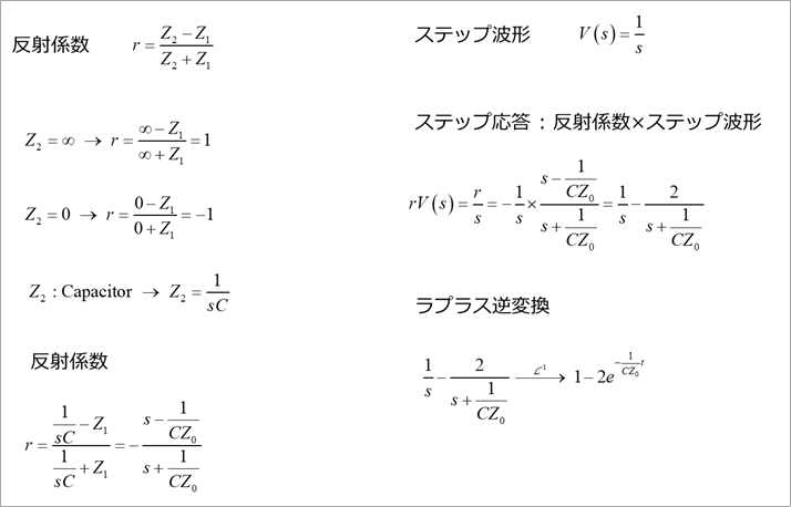
The formula in the sentence is hard to see, so I wrote only the formula collectively.
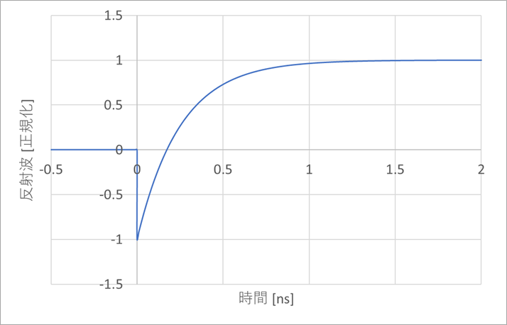
Figure 1 shows the reflected waveform of this step response.
C=5pF was chosen to exaggerate the effect of capacitive reflections.
This reflected wave travels to the other side of the track.
actual circuit
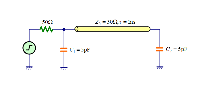
Figure 2 is an actual circuit for analyzing capacitive reflection. A generous capacitance of 5pF is used to highlight the effect of capacitive reflection.
The rise time of the signal source was set to 0.1ns. Almost step response.
The waveforms were analyzed with and without near-end capacitance C1 and far-end capacitance C2.
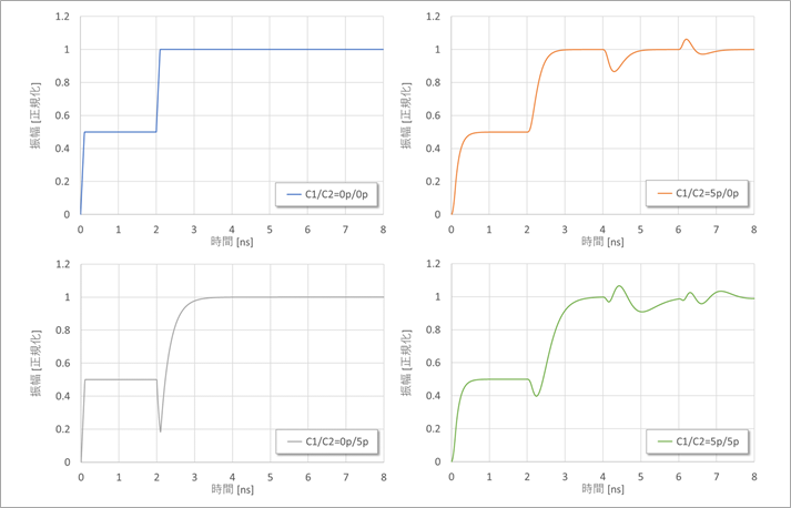
Figure 3 shows the near-end waveform.
In the upper left, C1/C2=0p/0pF, naturally there is no capacitive reflection.
C1/C2=5pF/0pF in the upper right is the roundness of the waveform due to C1 and the open reflection at the far end arriving at the near end, undergoing capacitive reflection, and then returning after being open-reflected at the far end. Capacitive reflection is observed at 4τ, ie two round trips.
The lower left C1/C2=0pF/5pF has the same shape as the reflected waveform of the step response waveform in Fig.1. The capacitive reflection at the far end is what arrives at the near end.
Bottom right, C1/C2=5pF/5pF is the superimposed near-end and far-end capacitive reflections.
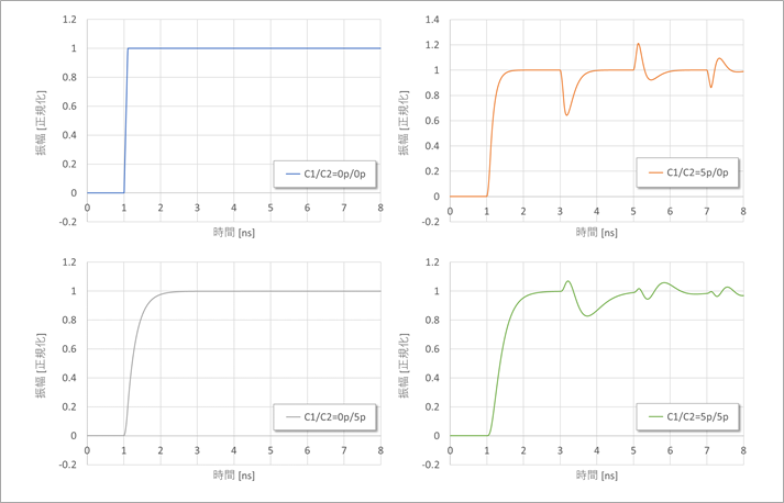
Figure 4 is the far end waveform.
In the upper left, C1/C2=0p/0pF, naturally there is no capacitive reflection.
In the upper right, C1/C2=5pF/0pF, the open reflection at the far end arrives at the near end, undergoes capacitive reflection, and returns after being open-reflected at the far end.
Bottom left, C1/C2=0pF/5pF is only waveform rounding due to C2 at the far end.
Capacitive reflections at the far end do not return to the far end because the near end is matched.
Bottom right, C1/C2=5pF/5pF is the superimposed near-end and far-end capacitive reflections.
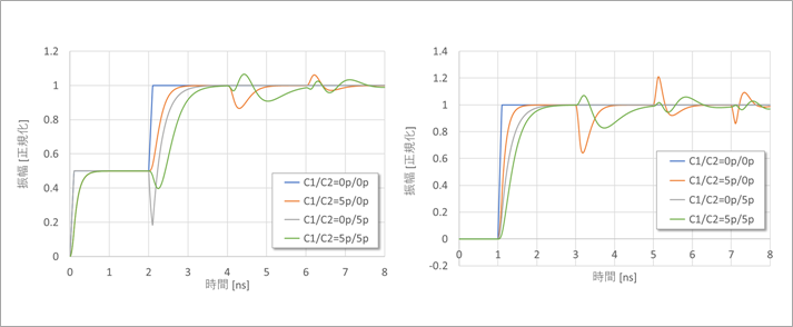
Figure 5 shows these waveforms overlaid.
Compare the waveform roundness for each waveform in Figures 3 and 4.
For the waveforms in Figures 3 to 5, C was chosen as large as 5 pF to clearly show the effect of capacitive reflection, as mentioned above.
As C decreases, the effect of capacitive reflection also decreases.
This capacitive reflection does not have a large change in amplitude, so it is unlikely that this itself will cause a malfunction.
Such noise, including but not limited to capacitive reflections, can shave timing margins.
To verify this, consider the far-end waveform when C1/C2 = 5pF/0pF, where capacitive reflection is most pronounced. This is the case in the upper right of Figure 4.
Capacitive reflection appears 2ns after the rise, that is, 2τ after the round trip of the line.
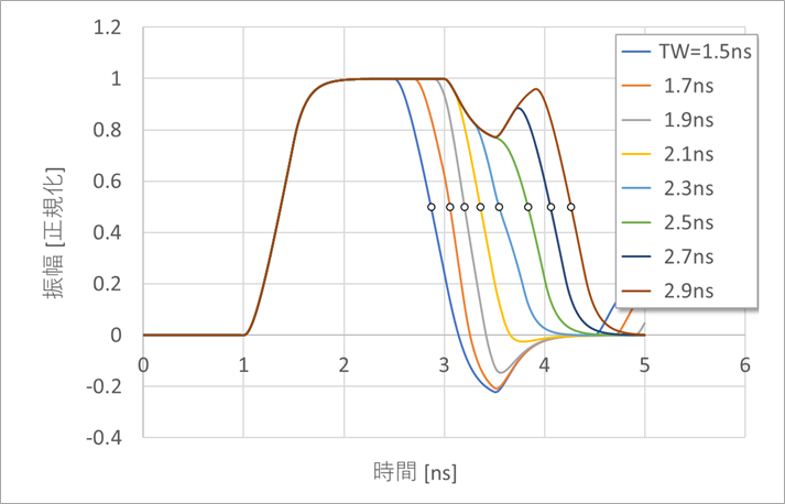
Figure 6 overlays the far-end waveforms with varying pulse widths. The circle (○) indicates the timing of the 0.5 amplitude when defining the pulse width.
The pulse widths at this time are evenly spaced 0.2ns increments, but the 0.5 amplitude timings are not even.
The pulse width seems to increase around TW=2.5ns in the figure.
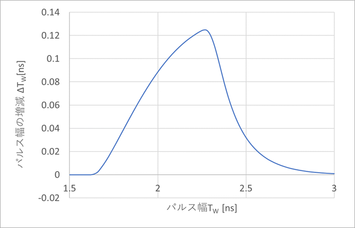
Figure 7 plots this increase or decrease (in this case only increase) in pulse width TW versus TW.
Around TW=2.3ns, the pulse width increases by about 0.12ns.
Here, we evaluated by increasing/decreasing the pulse width, but in reality, we cut the timing margin.
It should be noted that noise on the amplitude axis appears as a timing margin.
References
Yuzo Usui: All About Distributed Constant Circuits for Board Designers (3rd Edition) Self-published, pp.57-58, 2016
What is Yuzo Usui's Specialist Column?
It is a series of columns that start from the basics, include themes that you can't hear anymore, themes for beginners, and also a slightly advanced level, all will be described in as easy-to-understand terms as possible.
Maybe there are other themes that interest you!