- Semiconductor BusinessHOME
- Products and Services of Macnica,Inc.
-
technical information

-
Events and Seminars
- Handling Manufacturer
- Support
- Inquiry
- Click here to purchase products
- Semiconductor business e-mail magazine registration
![]()
![]() Narrow down by specifying conditions
Narrow down by specifying conditions
現在2171件がヒットしています。check
Line where Z0 changes midway due to wiring from BGA etc.
The wiring pattern under the BGA package and other wiring patterns have different wiring widths, so the characteristic impedance is different. As a result, waveform disturbance occurs due to reflection at the connection.
Width of pattern
The traces on the bottom of the BGA package must be threaded through the narrow gaps between the package terminals.
Since the pin density of BGA packages is high, the wiring pattern must inevitably be as thin as possible compared to normal wiring.
A thin wiring pattern has a high probability of disconnection, so it should be kept to the minimum necessary to avoid a decrease in yield.
For normal wiring patterns other than the bottom of the package, use a pattern width that is thicker (broader) than the bottom of the BGA, which provides sufficient yield.
characteristic impedance
The characteristic impedance of the wiring pattern is affected by the wiring width. Thin traces have high characteristic impedance and thick traces have low impedance.
Therefore, the BGA bottom has a high characteristic impedance, otherwise it is lower.
Wiring other than the bottom of the BGA is usually selected to be about 50Ω.
See below.
How to determine the characteristic impedance of a board
https://www.macnica.co.jp/business/semiconductor/articles/basic/111385/
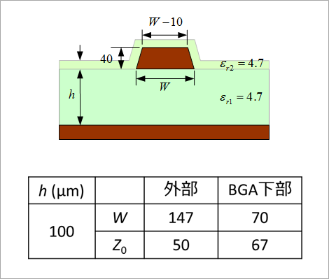
Figure 1 shows a cross section of the surface layer.
If the distance (thickness) h from the ground is 100μm and the pattern width at the bottom of the BGA is 70μm, the characteristic impedance Z0 is 67Ω.
Select Z0=50Ω except for the lower part of the BGA. The pattern width at this time is 147 μm.
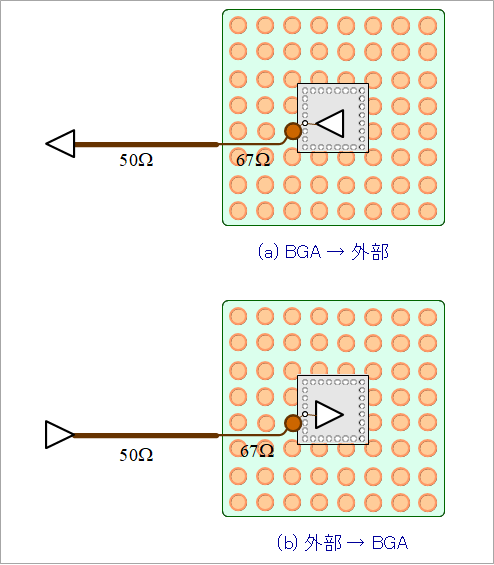
Figure 2 shows the wiring for this theme.
Because the characteristic impedance of the bottom of the BGA is different from that of the rest, there is an effect due to reflection at the connection point.
In (a) of the same figure, the BGA side is the driver, and the signal is transmitted from the BGA to the outside via a thin pattern. In (b) of the figure, conversely, a signal is transmitted from the outside to the BGA.
reflection analysis
In reflection analysis, the computational method obtains the waveform by fast Fourier transforming a grid diagram or a vertical sequence.
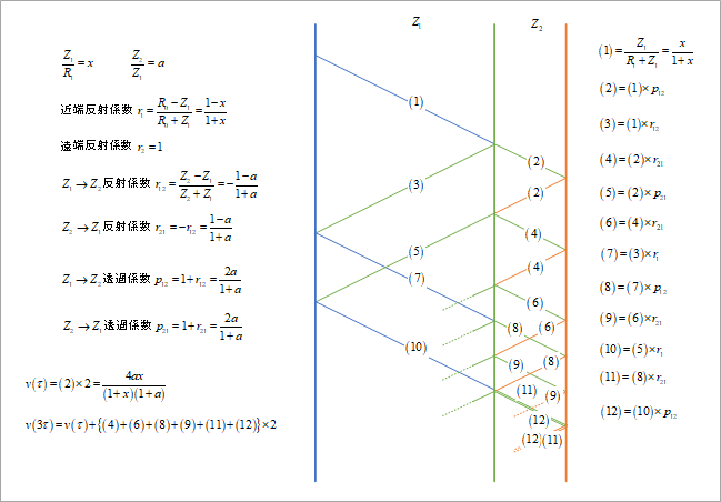
Figure 3 shows the grid diagram for Figure 2(b).
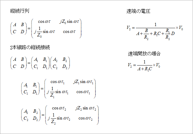
Figure 4 shows the calculation with vertical columns. V0 is the output swing of the driver.
Find the vertical sequence for the frequency and find the output waveform by iFFT (Inverse Fast Fourier Transform).
Calculations are useful to know the effect of each parameter, but SPICE is easier to just get the result.
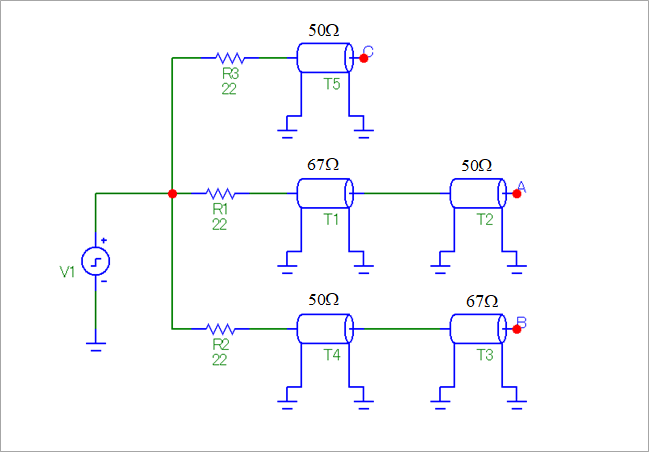
Figure 5 is an example schematic. Simultaneous analysis can be performed including (a) and (b) in Fig. 2 and the case where Z0 remains 50Ω and does not change during the process.
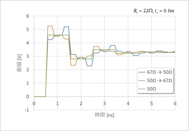
Figure 6 shows the waveforms at the far end (receiver end) under the conditions in Figure 2.
In the legend, 67Ω→50Ω corresponds to Fig. 1(a), and 50Ω→67Ω corresponds to Fig. 1(b).
Similarly, 50Ω is when the impedance is 50Ω without changing along the way.
The driver output resistance R1 is 22Ω, equivalent to a 12mA driver.
The green 50Ω waveform has a 4.5V overshoot and bounces around 2.8V.
On the other hand, a line whose impedance changes along the way causes even greater overshoot and bounce, as shown in the figure.
The figure shows the results of analysis using a vertical sequence and iFFT. Naturally, SPICE has the same result.
measures
As a countermeasure, insert a damping resistor of 22Ω, which is slightly larger than usual.
When R1=22Ω and Z0=50Ω, x=50/22=2.27. Adding a 22Ω damping resistor halves x=50/44=1.14 and x/(1+x) is reduced from 0.69 to 0.53.
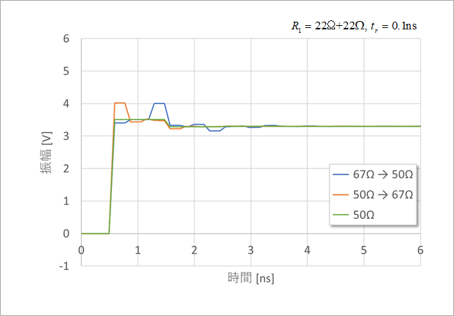
Fig. 7 shows the reflected waveform when a damping resistor of 22Ω is added. It can be seen that the overshoot is reduced and the bounce is suppressed.
Typically, for a 12mA driver, the value of the damping resistor should be 18Ω for 10% overshoot and 11Ω for up to 20% overshoot.
How to find the damping resistance
"Easier determination of damping resistor value"
https://www.macnica.co.jp/business/semiconductor/articles/basic/112905/
Please refer to
In the case of Figure 2(a), the driver is a BGA, so no damping resistor can be inserted. If this IC is an FPGA, select a low drive capability.
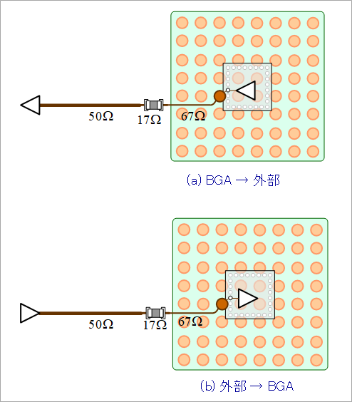
As another countermeasure, as shown in Fig. 8, a method of inserting 17Ω (16Ω or 18Ω for the E24 series) of this impedance difference at the connection point between the 67Ω line at the bottom of the BGA and the external 50Ω line. there is.
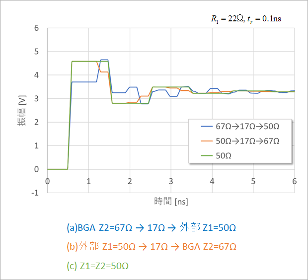
Figure 9 shows the analysis results at this time.
Both the overshoot and its rebound are within the range of 50Ω.
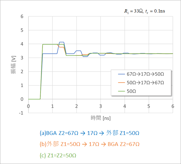
Furthermore, it is the analysis result when a damping resistor of 11Ω is inserted in Fig. 9 (R1 = 33Ω).
I have suggested some workarounds.
Select the most effective countermeasure by comparing the presence or absence of an external resistor and the effectiveness of countermeasures.
What is Yuzo Usui's Specialist Column?
It is a series of columns that start from the basics, include themes that you can't hear anymore, themes for beginners, and also a slightly advanced level, all will be described in as easy-to-understand terms as possible.
Maybe there are other themes that interest you!