- Semiconductor BusinessHOME
- Products and Services of Macnica,Inc.
-
technical information

-
Events and Seminars
- Handling Manufacturer
- Support
- Inquiry
- Click here to purchase products
- Semiconductor business e-mail magazine registration
![]()
![]() Narrow down by specifying conditions
Narrow down by specifying conditions
現在2183件がヒットしています。check

After working at a machine manufacturer for three and a half years, working on development work such as housing and mechanism design, I joined Macnica mid-career as an FAE.
Macnica has a large proportion of mid-career employees, so it's very easy to work here and you don't feel alienated at all.
Originally, I studied mechanics at university and had no knowledge of electricity at all when I joined the company, so I started over from Ohm's law and am currently studying desperately.
I had an opportunity to actually design a DC/DC converter under such circumstances, so I hoped it would be helpful for a beginner electrician like myself.
I would like to introduce the process.
This article is created using a printed circuit board, using the same circuit diagram as in the "I tried to make a DC/DC converter using a universal board" edition.
Creating a schematic
In the previous article “I tried making a DC/DC converter using a universal board. The result of the challenge was,
It worked pretty well, but I'm going to do my best and believe that it will be even better this time!
The circuit diagrams are basically the same.
This time, we used surface mount components as much as possible to replicate a real application.
The surface mount type is also called SMD (Surface Mount Device).
This type has become the mainstream of circuit boards in the real world, and is becoming smaller and available in a variety of sizes.
First of all, to make a printed circuit board, you need to prepare special software.
KiCAD that can be used for free this time KiCad EDA - Schematic Capture & PCB Design Software I used
The first thing to do after starting KiCAD is to create a circuit diagram!
This needs to be done to reflect the connection relationships between parts, the size of parts, etc.
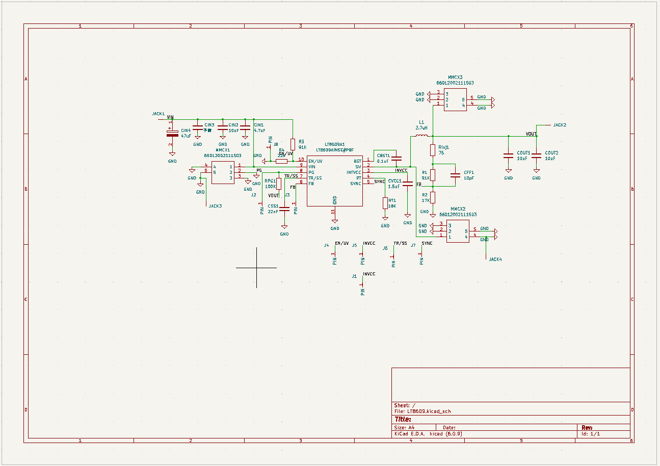
Something like this.
At first glance, the circuit diagram looks like it was drawn with LTspice, but since it is a board creation tool, it can be converted into a component model.
"Footprint data" is linked.
Footprint data includes the shape of the copper foil part (land pattern) for soldering parts, etc.
Contains the part name for printing.

The land pattern differs depending on the parts used, so it is necessary to obtain each part separately.
*Capacitors etc. are determined by standards such as 1005 size, so if you choose footprint data of the same size, it is OK.
Macnica-Mouser also allows you to download footprint data.
If the part page says "ECAD model", footprint data is also available here.
This obtained model can be loaded into KiCAD using a tool called Library Loader.
Creating a board pattern
Now that the preparations are complete, let's create the board pattern.
So, even though I have no know-how about circuit board pattern design, here is the pattern I wrote using all my knowledge.
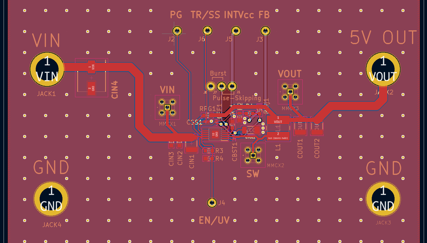
If someone with knowledge of circuit board patterns saw this layout, it would probably make them faint (lol).
Even with this, I had a lot of trouble writing it as I was just trying to figure it out.
Next time, I won't be able to continue like this, so I will ask my senior colleagues at work to review it and make improvements.
Universal board/printed circuit board list
■Universal board edition
・ I made a DC/DC converter using a universal board (1)
・ I tried making a DC/DC converter using a universal board (2)
・ I tried making a DC/DC converter using a universal board (3)
・ I made a DC/DC converter using a universal board (4)
■Printed circuit board edition
・Make a power supply with your own printed circuit board! (1)
・ Create a power supply with your own printed circuit board! (2)
・ Create a power supply using a homemade printed circuit board! (3)
・ Create a power supply using a homemade printed circuit board! (4)
・ Create a power supply using a homemade printed circuit board! (5)