- 半導体事業HOME
- マクニカの製品・サービス
-
技術情報

-
イベント・セミナー
- 取扱メーカー
- サポート
- お問い合わせ
- 製品購入はこちら
- 半導体事業のメルマガ登録
![]()
![]() 条件を指定して絞り込む
条件を指定して絞り込む
現在2004件がヒットしています。check

私は機械メーカ―で3年半、筐体や機構設計など、開発業務に携わった後、マクニカにFAEとして中途入社しました。
マクニカは中途入社の方の比率も多く、全く疎外感がなくとても過ごしやすいです。
もともと、大学も機械系で入社時には全く電気の知識がなく、オームの法則からやり直し現在、必死に勉強中です。
そんな中で実際にDC/DCコンバーターを設計する機会がありましたので、私のような電気屋初心者の方の手助けになればと
その過程をご紹介させていただきます。
今回は第2稿目です。第1稿目はこちらからご覧ください。
いざ動作確認
今回作成した基板の電源を入れます。要求仕様は以下です。
・入力電圧 :6~36V (TYP.12V)
・出力電圧 :5V
・出力電流 :2A
負荷2Aで入力電圧を6Vから徐々に上げ、動作確認をおこないました。
出力5Vは出ていたのですが、入力電圧を16Vにあげたところでデバイスからパチッと音がして出力が出なくなってしまいました。
このことを先輩社員に相談すると、いきなりフルパワーの負荷2Aで確認するべきではなかったと。まず無負荷動作などデバイスにかかる負荷が
小さいところから評価するべきだとアドバイスをいただきました。
この時はまずは動作確認といった軽い気持ちでデバイスを動かしてしまったため、なぜ壊れたのか判断材料となる波形データなどをとっていませんでした。
電気の世界では、壊れた後ではなにが起こっていたか、どこが壊れたのか検証が大変だということを実感しました。
だからこそ、動作中の波形等データを常にとっておく癖をつけることは電気屋さんとして大事だと学びました。
破損原因の確認
デバイスが壊れてしまった可能性が高いため、デバイスを変換基板ごと換装しました。
入力電圧16Vで出力電圧5V/電流2Aでデバイスが破損してしまったため、入力電圧12Vとして出力電圧5V/電流1Aに抑え、波形を観察しました。
スイッチ(SW)周期がたまに乱れてしまうことに加えて、入力電圧12V に対して、SW時のスパイク最大電圧が28Vにも達していました。データシートの参考スイッチ波形は入力電圧に対して+5V程度ですので、これは明らかに大きすぎます。
もし、この波形の電圧が本当に印加されているのだとしたら、電圧・負荷電流を増加させるとデバイスの絶対定格である42Vを超えた電圧がかかる恐れがあると考えられ、まずこのスパイクノイズを除去することに注力しました。
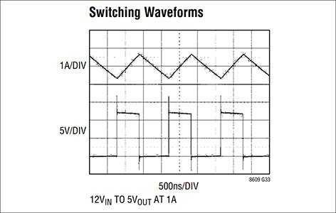
データシートの参考波形
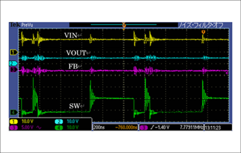
観測波形 ①VIN電圧 ②VOUT電圧 ③FBピン電圧 ④SWピン電圧
SW波形の乱れ・スパイクノイズの原因を探る
なぜSW波形が乱れてしまったり、スパイクノイズが観測されるのでしょうか。
まず、最初に試したのが入力コンデンサー(CIN)の位置変更です。
CINはデータシートにはできるだけデバイスの近くに置くことと記載されていますが、今回変換基板を噛ませていた関係でどうしても位置が遠くなってしまっていました。
デバイス変換基板へ、少し無理やり感は否めないですが移植しました。

CINコンデンサーの移動
再測定
再測定してみましょう。
結果はどうでしょう。スパイクのピーク電圧は22Vで、CIN移動前と比較して6Vほど低減されています。
移動前に見られていたSW波形の乱れもなくなり安定動作させることができました!

CIN移植後の観測波形 ①VIN電圧 ②VOUT電圧 ③SWピン電圧 ④FBピン電圧
なぜCINを近づけると良いのでしょうか?
回路上の銅線やパターンには寄生抵抗と寄生インダクタンス成分が含まれていて、これらがノイズの原因となりえるのです。
入力コンデンサーCINは、これらのノイズを除去する役割がありますが、デバイスから遠いと意味を成さなくなってしまうのですね。
できるだけ近くに配置とデータシートには記載されていましたが、これほどまでに近づけなくてはならないのか、、といい勉強になりました。
CINの移動によって、スパイク電圧は多少改善されましたがまだ大きすぎます。このままでは入力電圧を上げるとデバイスの定格に抵触してしまいそうです。
次回はスパイクの改善についてもっと深堀してきます。
お楽しみに。
ユニバーサル基板編記事一覧
■ユニバーサル基板編
・ユニバーサル基板でDC/DCコンバーターを作ってみた (1)
・ユニバーサル基板でDC/DCコンバーターを作ってみた (2)
・ユニバーサル基板でDC/DCコンバーターを作ってみた (3)
・ユニバーサル基板でDC/DCコンバーターを作ってみた (4)
■プリント基板編