- Semiconductor BusinessHOME
- Products and Services of Macnica,Inc.
-
technical information

-
Events and Seminars
- Handling Manufacturer
- Support
- Inquiry
- Click here to purchase products
- Semiconductor business e-mail magazine registration
![]()
![]() Narrow down by specifying conditions
Narrow down by specifying conditions
現在2168件がヒットしています。check

After working at a machine manufacturer for three and a half years, working on development work such as housing and mechanism design, I joined Macnica mid-career as an FAE.
Macnica has a large proportion of mid-career employees, so it's very easy to work here and you don't feel alienated at all.
Originally, I studied mechanics at university and had no knowledge of electricity at all when I joined the company, so I started over from Ohm's law and am currently studying desperately.
I had an opportunity to actually design a DC/DC converter under such circumstances, so I hoped it would be helpful for a beginner electrician like myself.
I will introduce the process.
This is the third draft; please see the second draft here.
Review of measurement method
Last time, I succeeded in suppressing the spikes in the SW waveform by moving the input capacitor (CIN).
However, the spikes in the SW waveform were still large, and I doubted whether the waveform I was seeing was the true waveform.
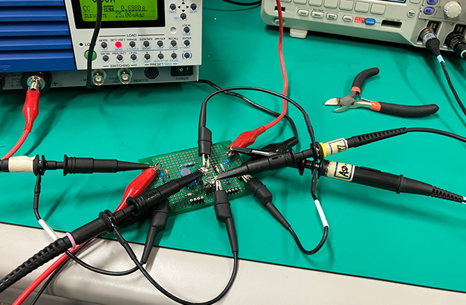
Initially, measurements were taken with a regular probe attachment, but will be changed to measurements with an MMCX connector.
Although it takes time and effort to mount the MMCX connector on the board, if a suspicious waveform appears, check the cause of measurement error.
I learned that it is important to measure while excluding as much as possible, so I decided to give it a try.
Measurement with normal probe
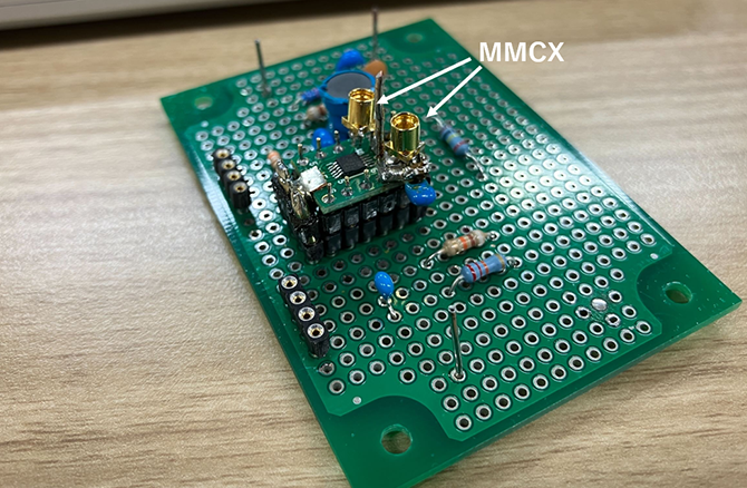
Mounted MMCX connector
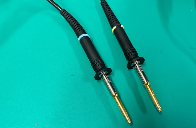
MMCX conversion connector attached probe
With normal probes, the GND wiring is long and the parasitic inductance component becomes large, but by using an MMCX connector, this loop can be made extremely small, making it less susceptible to measurement errors.

Regular probe attachment and MMCX attachment
Let's compare the waveforms when changing to the MMCX connector.
MMCX connector was implemented on the input node and SW node.
*Since the probe compatible with the MMCX attachment could not be used with the previous oscilloscope, we have changed to a new oscilloscope.

Measurement with MMCX connector
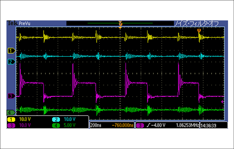
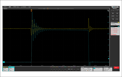
Measured waveform with normal probe attachment (CH1:VIN CH2:VOUT CH3:SW CH4:FB)

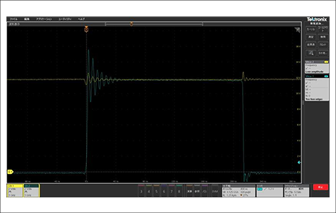
Measured waveform at MMCX connector (CH1:VIN, CH2:SW)
The spike voltage at the SW node was observed to be lower than when pinched with a normal probe.
It changes from 28V to about 18V.
I was surprised that there was a difference of 10 V depending on the measurement method.
By the way, I also tried a method of measuring by attaching a GND spring to the normal probe, but
The spike voltage at the SW node was observed at 19V, with the MMCX connector giving the best results.
Looking at this result, I want to acquire the waveform with the MMCX connector at all costs,
It was also difficult to implement the connectors, so it was not realistic to use MMCX connectors at all measurement points every time we made a measurement.
I learned that it is important to identify important points and use measurement tools such as MMCX.
Please also refer to the article below for information on the effects of probing methods on measurements.
Does the ripple voltage double due to different probes and accessories? !
Adding an input capacitor
We noticed that the VIN waveform contained noise that correlated with the SW waveform at the switching timing.
Normally, this kind of VIN noise is absorbed by the input capacitor, but I thought it might not be absorbed completely.
Currently, only 4.7 μF x 1 input capacitor is installed.
Let's try adding a 1.0 μF capacitor.
Before adding input capacitor 1uF (CH1:VIN, CH2:SW)
After adding input capacitor 1uF (CH1:VIN, CH2:SW)
The waveform of the input voltage (VIN) is so clean that you can hardly recognize it!
At the same time, the spike noise of the SW waveform has been reduced, and we were able to bring it to a level comparable to the data sheet value.
Now, even if it is operated with an input voltage of 36V, there is no risk of exceeding the rating due to a spike on the SW node.
Next time, we will perform performance measurements against the required specifications.
Is it possible to meet the required specifications?
looking forward to!
Universal board edition article list
■Universal board edition
・ I made a DC/DC converter using a universal board (1)
・ I tried making a DC/DC converter using a universal board (2)
・I made a DC/DC converter using a universal board (3)
・ I made a DC/DC converter using a universal board (4)
■Printed circuit board edition
・ Create a power supply with your own printed circuit board! (1)
・ Create a power supply with your own printed circuit board! (2)
・ Create a power supply using a homemade printed circuit board! (3)
・ Create a power supply using a homemade printed circuit board! (4)
・ Create a power supply using a homemade printed circuit board! (5)