- Semiconductor BusinessHOME
- Products and Services of Macnica,Inc.
-
technical information

-
Events and Seminars
- Handling Manufacturer
- Support
- Inquiry
- Click here to purchase products
- Semiconductor business e-mail magazine registration
![]()
![]() Narrow down by specifying conditions
Narrow down by specifying conditions
現在2189件がヒットしています。check

After working at a machine manufacturer for three and a half years, working on development work such as housing and mechanism design, I joined Macnica mid-career as an FAE.
Macnica has a large proportion of mid-career employees, so it's very easy to work here and you don't feel alienated at all.
Originally, I studied mechanics at university and had no knowledge of electricity at all when I joined the company, so I started over from Ohm's law and am currently studying desperately.
I had an opportunity to actually design a DC/DC converter under such circumstances, so I hoped it would be helpful for a beginner electrician like myself.
I will introduce the process.
This article is created using a printed circuit board, using the same circuit diagram as in the "I tried to make a DC/DC converter using a universal board" edition.
Board pattern review
Last time I wrote the board pattern the way I wanted it, but this time I would like to have it reviewed.
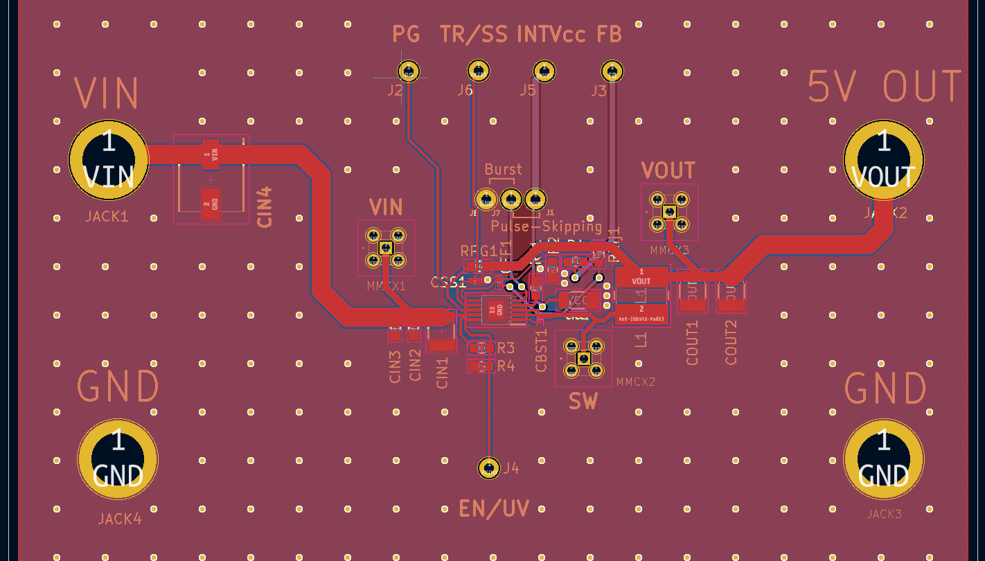
First board pattern I drew
After many revisions and reviews, the final board layout looks like this.
Board pattern after review
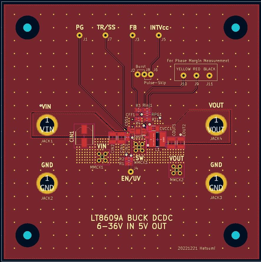
You looked wrong! (lol)
I think there is still room for modification, but for now, this is the decision.
What was wrong with changing so much? . That being said, I have summarized the main corrections below.
Main fixes
- Input/output nodes are too narrow. Parasitic resistance and inductance may cause the voltage to drop (voltage drop) or cause noise.
This may occur.
・How to arrange input capacitors
Cut in order from the lowest frequency, and finally use the capacitor with the smallest capacity, that is, the capacitor for cutting the highest frequency.
Get as close to the device's PIN as possible.
・Important capacitors such as Css and INTVcc, which are stated in the data sheet to be placed close to the device, should be placed as close as possible.
・Hot loops are separated by other patterns. Do not place any obstacles on the hot loop.
・How to take the voltage FB point
The point to monitor the output should be the most stable point.
- The SW node (the connection between the SW pin of the power supply IC and the inductor) should be made as wide as possible.
Impressions after board review
I learned that being conductive and functioning as a pattern are two completely different things.
All pattern wiring that connects components (including the solid GND) contains parasitic inductance and resistance components, which must be taken care of. And what is the part that needs to be taken care of? I thought it was important to have a clear understanding of this.
To be honest, I wasn't really aware of the flow of current, so I thought it was important to always be aware of it from now on.
Also, if you look at the Analog Devices product page, you may be able to download the evaluation board layout.
The evaluation board has an ideal design, so I thought I could save some time by referring to it.
Ordering the board
However, it is difficult to know whether the difference between the patterns actually appears because I have never experienced it.
I decided to order both the pre-review and post-review patterns and compare them.
Once we have finalized the pattern, we will begin ordering.
I ordered the board from a site called Elecrow Elecrow: PCB Prototype & Open Hardware For Makers. This is a super cheap site where you can make a two-layer board for around 100 yen each. . .
Can you make money with this? I'm worried though (lol)
The detailed steps are too long to explain here, but after outputting Gerber data with KiCAD, files are generated for each layer.
It was OK if I converted it to the extension specified by Elecrow and uploaded the data.
Next time, we will mount and evaluate the components on the board we received!
Universal board/printed circuit board list
■Universal board edition
・ I made a DC/DC converter using a universal board (1)
・ I tried making a DC/DC converter using a universal board (2)
・ I tried making a DC/DC converter using a universal board (3)
・ I made a DC/DC converter using a universal board (4)
■Printed circuit board edition
・ Create a power supply with your own printed circuit board! (1)
・Create a power supply with your own printed circuit board! (2)
・ Create a power supply using a homemade printed circuit board! (3)
・ Create a power supply using a homemade printed circuit board! (4)
・ Create a power supply using a homemade printed circuit board! (5)