- Semiconductor BusinessHOME
- Products and Services of Macnica,Inc.
-
technical information

-
Events and Seminars
- Handling Manufacturer
- Support
- Inquiry
- Click here to purchase products
- Semiconductor business e-mail magazine registration


 Narrow down by specifying conditions
現在2240件がヒットしています。check
* Please see below for the contents up to this point.
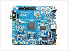
Beryll's FPGA flashes by clock synchronization! [#1/3]
Beryll's FPGA flashes by clock synchronization! [#2/3]
Let's write the design we have actually designed on the Beryll board and make it work.
6. Debug the actual machine
I would like to use the Cyclone® V GX's JTAG port to transfer configuration data (*.sof) directly from my computer for debugging.
After attaching the power cable to Beryll, connect Beryll and the computer with the included USB-miniUSB cable, and turn on the power of Beryll.
Launch the Quartus® Prime Programmer, set the SOF file, and click the Start button♪ When the Progress bar of the Programmer reaches 100%, the data transfer is complete.

When connecting to Beryll for the first time, a driver must be installed to recognize the On-Board USB-Blaster.
Please see this article for installation instructions.

Here we go! Verification on actual machine
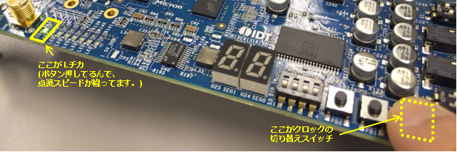
You can see the LED blinking.
Now, let's press the push button to switch the input clock frequency of the register inside the FPGA.
Oh! Flashing speed changed! (Sorry, it's a still image.)
7. Program into configuration ROM
Now that debugging is complete, write the Cyclone® V configuration data to the on-board configuration ROM (EPCS128) using the Quartus® Prime Programmer.
The method of data transfer between Cyclone® V and EPCS devices is called "active serial configuration mode (commonly known as AS mode)." Typically, programming an EPCS device using this AS interface requires a 10-pin header on the board (the header on the left in the figure below). Attach the USB-Blaster II or USB-Blaster download cable connector to this header.
On the other hand, if you configure data to the FPGA via the JTAG port as in operation 6 above, or use the FPGA debug function called SignalTap® II, you need to separately connect the 10-pin header for JTAG to the FPGA. (header on the right side of the image below) is also required.
With this, you have to reserve space for two 10-pin headers on the board, right?
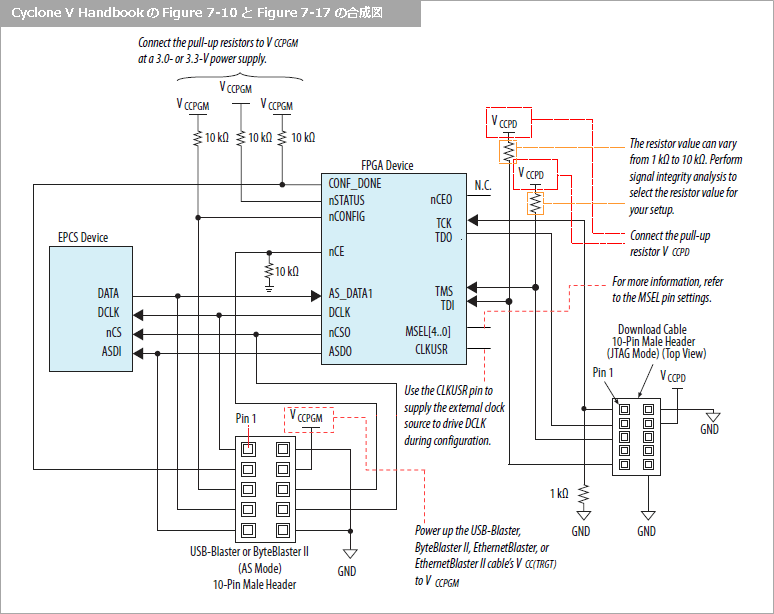
However, by leveraging the JIC(JTAG Indirect Configuration) feature, the FPGA's internal serial flash loader (SFL) design can be bridged to allow programming of the EPCS device through the JTAG port. This eliminates the need to prepare a 10-pin header for AS mode, reducing board area and lowering costs.
[Reference] AN 370: Using the Intel FPGA SerialFlash Loader with the Intel Quartus Prime Software
Beryll employs exactly this configuration.
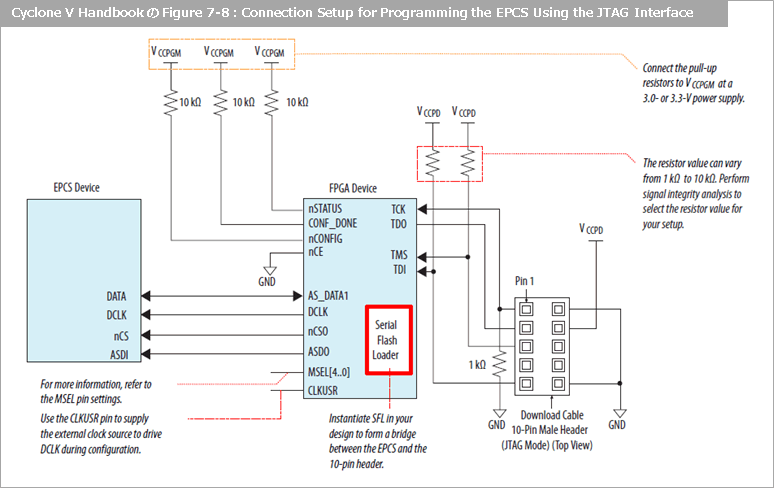
Programming via the serial flash loader is done with a JIC file instead of the traditional SOF and POF files. Create a JIC file from the SOF file of the configuration file for FPGA and execute programming.
The operation flow consists of the following two steps.
7-1. Generate JIC file from SOF file
7-2. Programming to EPCS
7-1. Creating a JIC file
(1) Select File menu > Convert Programming Files.
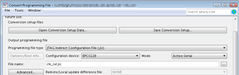
(2) Select and specify the following contents in the Output Programming File item.
- Programming file type: JTAG Indirect Configuration File (.jic)
- Configuration device: EPCS128 (model of configuration device to program)
- Mode: Active Serial
- File name: Select the save folder for the generated file and specify the output file name
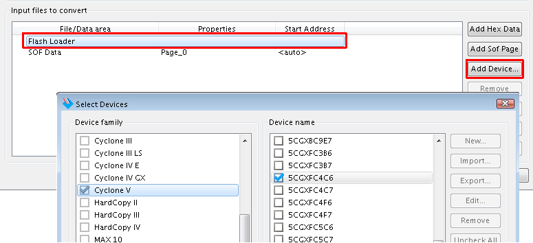
(3) Select and specify the following contents in the Input files to convert item.
(3)-1. Select the type of FPGA that uses the serial flash loader design.
- Select the Flash Loader line and click the Add Device button.
- Select Device dialog Box: Device family= Cyclone V, Device name= 5CGXFC4C6
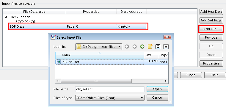
(3)-2. Specify the configuration file (.sof) that is the basis of the JIC file.
- Select the SOF Data row and click the Add File button.
- Select the sof file to convert and click the Open button.
To compress programming files, select the SOF file you want to compress and click the Properties button. In the SOF File Properties dialog Box, check the Compression option and click the OK button.
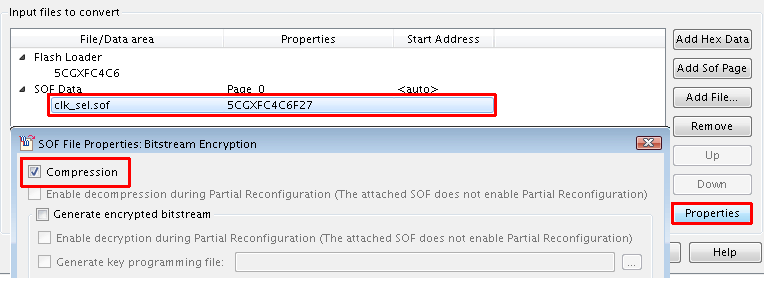
(4) Click the Generate button.
The message “Generated jic file name successfully” is displayed and JIC file generation is completed.
7-2. Programming to EPCS
Program the generated JIC file into the EPCS device in JTAG mode.
Start the Quartus® Prime Programmer. After setting the JIC file and checking the Program/Configure option, click the Start button.When the Progress bar in the Programmer reaches 100%, you have finished programming the EPCS device with the JTAG Indirect Configuration.
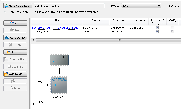
Every time I power up the Beryll board, the EPCS128 transfers the configuration data to the Cyclone® V GX FPGA and the FPGA starts working.
This time, in addition to introducing Beryll, I sent various information necessary for FPGA development.
Please use it for your own development.
Beryll's FPGA flashes by clock synchronization! series
Beryll's FPGA flashes by clock synchronization! [#1/3]
Beryll's FPGA flashes by clock synchronization! [#2/3]
Beryll's FPGA flashes by clock synchronization! [#3/3]
Beryll developer interview
This is how Beryll was created! - Asking the Development Leader -
Related products