- 半導体事業HOME
- マクニカの製品・サービス
-
技術情報

-
イベント・セミナー
- 取扱メーカー
- サポート
- お問い合わせ
- 製品購入はこちら
- 半導体事業のメルマガ登録


 条件を指定して絞り込む
現在2213件がヒットしています。check
※ ここまでの内容は以下をご覧ください。
Beryll の FPGA でクロック同期によるLチカ![#1/3]
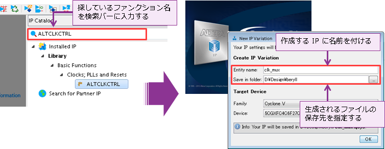
ALTCLKCTRL は Cyclone® V GX をサポートしているので、早速 Quartus® Prime の IP Catalog(Tools メニュー)で作成しましょう!
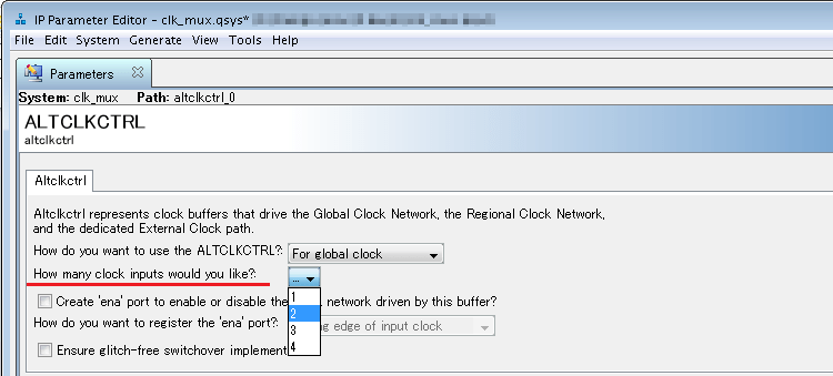
パラメータ画面で、ALTCLKCTRL の機能を設定します。このデモのパターンBでは、2つのクロック入力を選択するので、「How many clock inputs would you like?」= 2 とします。(他はデフォルト)
Generate HDL ボタンをクリックし、Synthesis セクション(「Create HDL design files for synthesis:」)および Simulation セクション(「Create simulation model:」)で生成する HDL 言語タイプをそれぞれ選択します。
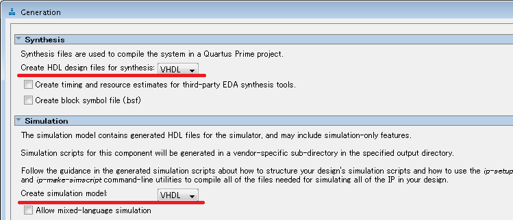
Generate ボタンをクリックし、「Generate: completed successfully.」が表示されたら Finish ボタンをクリックして ALTCLKCTRL の完成です。これを自分のトップ階層のデザインに組み込みます。

IP Catalog でコアを生成すると、保存先に指定したフォルダ内にその IP 名のフォルダが作成されていて、中には上位階層でインスタンスするための補助ファイル(*_inst.vhd/*_inst.v)があります。これらを活用してユーザー回路に接続すると簡単です。
ALTCLKCTRL の詳細はこちらのユーザーガイドをご覧ください
ClockControl Block (ALTCLKCTRL) IP Core User Guide

さて、話を本題に戻しましょう。
2つのデザインをコンパイル(ピン・レイアウトは固定)してみた結果がコチラです。
| パターンAの回路 | パターンBの回路 | |
| レジスタ数(フリップフロップ) | 83 | 48 |
| ALM(Adaptive Logic Module) | 48 | 30 |
| Fmax: CLK0(50MHz) | 236.74 MHz | 173.88 MHz |
| Fmax: CLK1(125MHz) | 223.46 MHz | 249.69 MHz |
このとおり、論理的には同じ動作を実現できるデザインであっても、ロジック構成や記述方法によって FPGA に実装されるとリソースやスピードに差が生じます。今回の場合はどちらのパターンもクロックが要求値を大幅にクリアしていて、これ以上回路規模を拡大もしないのでどちらのパターンでも良いのですが、強いて言うならリソース使用率が大きいと言うことは消費電力にも影響しますので、少ないリソースで実現できるのであればそれが良いデザインと言えるでしょう。
今回のパターン B のように、ユーザーが自作で作る論理回路だけでなく、ターゲット・デバイスが保有している機能(DSP ブロック、メモリ・ブロック、PLL、トランシーバ、ARM など)を理解しうまく活用することで、効率の良い開発が目指せますよ。
2. 論理シミュレーションをする
自分で書いた論理回路を動作検証するためのテストベンチを書きます。
その後、ModelSim* - Altera® FPGA Edition(Starter Edition でも可)でシミュレーションします。

参考技術コンテンツ
はじめてみよう!テストベンチ
3. 制約を設定する
再び Quartus® Prime です。
3-1. ピンレイアウトおよび I/O 規格を設定
論理回路上の入力ピンと出力ピンに、デバイス上のピン番号を指定します。それと同時に、それらピンの I/O 規格も設定します。

Cyclone® V GX デバイスは、電源がトランシーバ・ブロック用と FPGA 用に分かれています。
その FPGA 側の電源は8ブロックに分かれていて、これを Altera® FPGA では I/O バンク と呼んでいます。
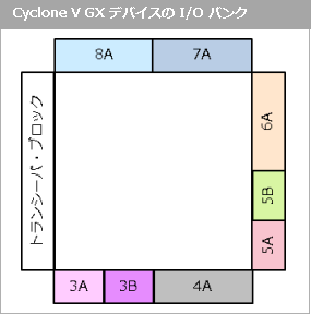
各 I/O ピンはいずれかの I/O バンクに属していて、その I/O バンク用の電源が供給されています。
各 I/O バンク用の電源は異なる電圧を供給することができるので、一つのデバイスで様々な I/O 規格をサポートでき、色々な IC とインタフェースを取ることができます。
ユーザーは “どの I/O バンクに何の I/O 規格を集結させるか” や、”この I/O バンクの電源は△ボルトにする予定だから、この I/O ピンをレイアウトできる” などとピンのレイアウトを自由に構成できます。
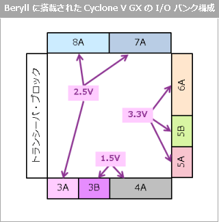
バンクがいくつ/どのように分割されているかはデバイス・ファミリで異なりますので、必ずデバイスのハンドブックやピンアウト・ファイルなどを確認してください。
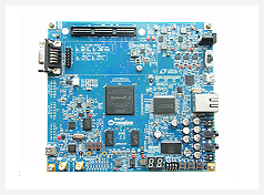
今回の Beryll ボードは評価ボードのため電源構成やピンレイアウトが決められています。

Beryll の基板仕様に合わせて下表のとおりピン番号と I/O 規格を設定していきましょう。
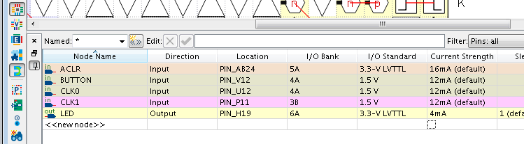
また、FPGA のユーザー I/O ピンは出力電流値を選択することができて、これも Quartus® Prime の Pin Planner で設定(オプション名: Current Strength)できます。出力電流は FPGA の消費電力や信号出力時のノイズに影響を及ぼしますので、コントロールできるのは嬉しいですね。
設定できる電流値はターゲット・デバイスや設定する I/O 規格により異なりますので、必ずご利用のデバイスのハンドブックを確認してください。
今回のデモにおいて、出力ピンは LED をドライブする1本のみで、しかも基板図をよく見ると H19 ピンは GND 出力時にLED が点灯する仕様です。High 出力時にはドライブ目的はありませんので、電流量は一番小さい 4mA にしていますが、デフォルトでも問題ありません。
3-2. 未使用のユーザー I/O ピンを特定の属性に予約設定
通常 ユーザー作成基板の場合には、使用していない各ユーザー I/O ピンが基板上でどのように処理されているかに応じて、Quartus® Prime でもそのピンに対して適切な属性でプログラムされるように設定をします。
例えば、ある未使用のユーザー I/O ピンが基板上はどこにも接続していない(未接続)ならば、Quartus® Prime ではそのピンに対して “内部ウィーク・プルアップ付きの入力” または “出力” として予約することになります。
設定方法や設定項目などの詳細は、「Quartus® Prime はじめてガイド - デバイス・オプションの設定方法」 および 「Quartus® Prime はじめてガイド - ピン・アサインの方法」 をご覧ください。
Beryll の場合は、8つのユーザー I/O ピン(AC10/T11/W11/Y11/AE10/AE13/Y15/G7)を除いたユーザー I/O ピンは何かしら接続されていますので、トライステート入力に予約します。

8つの未使用かつ未接続のユーザー I/O ピン(AC10/T11/W11/Y11/AE10/AE13/Y15/G7)は、今回 GND 出力に予約し、Beryll の電源仕様に応じた I/O 規格を設定します。
また Flash ROM/SRAM/DDR3 SDRAM は今回のデモでは使用しないので、各メモリ・デバイスのチップセレクト(CS)ピンをディセーブルにするために、Cyclone® VGX 側のピンを VCC 出力に予約し、I/O 規格、出力電流値を設定します。
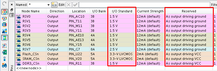
3-3. デバイスのピン・オプションを設定
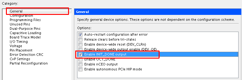
INIT_DONE ピン(U19番ピン)はオプション・ピンとして使用するように基板処理されているので、オプションを有効にします。
Assignments メニュー > Device > Device and Pin Options > General カテゴリ より
Enable INIT_DONE output = On
3-4. コンフィギュレーション・モードを選択
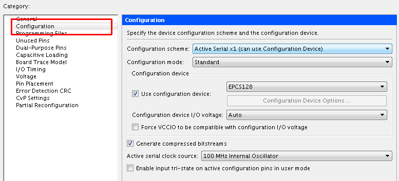
Beryll には Cyclone® V GX のコンフィギュレーション ROM として EPCS128SI16N が搭載されていて、かつ Cyclone® V GX の MSEL ピンは MSEL[4:0]=10011 に接続されています。
つまりデータ転送方式はアクティブ・シリアル・コンフィギュレーション・モード (AS モード) の仕様です。
今回は、
- Configuration scheme: Active Serial x1 (can use Configuration Device)
- Configuration mode: Standard
- Use configuration device = On / EPCS128
- それ以外はデフォルトのままにします。
3-5. 論理回路に対するタイミング制約を作成および登録
今回はクロック制御回路です。タイミング制約をするため、SDC ファイルを作成します。
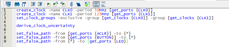
1行目、2行目はクロック定義です。
3行目はクロック・マルチプレクサ構成の制約コマンドです。
今回のデモの回路構成(パターンB)は、周波数の異なる2つのクロックをセレクトする構成です。50MHz のクロックでも 125MHz のクロックでも動作するかタイミング解析させる必要があります。でもクロックがセレクト後は 50MHz と 125MHz のクロックが同時に有効にはなりませんから、set_clock_groups コマンドの -exclusive オプションで制約します。
5行目はクロックのバラツキを自動計算してタイミング解析に反映させるためのコマンドです。
7~9行目はタイミング解析の対象から除外するためのコマンドです。
リセット信号(ACLR)やクロック切り替え信号(BUTTON)は、人がプッシュボタンを押して制御します。非同期入力であることや人が押すスピードを考えると、タイミング解析の必要はないので除外しました。
タイミング制約を作成後、Quartus® Prime の Assignments メニュー > Settings > TimeQuest Timing Analyzer で SDC ファイルを登録します。
4. コンパイルをする
コンパイルを実行するため、Start Compilation ボタンを ポチッ♪
これで論理合成と配置配線が実行されて、FPGA 内部で実行させるプログラム・データも同時に生成されます。
5. タイミング検証をする
コンパイル終了後に生成されたコンパイル・レポートにおいて、TimeQuest Timing Analyzer レポート箇所を確認し、タイミング制約で与えた条件を満たした結果になったかを検証します。
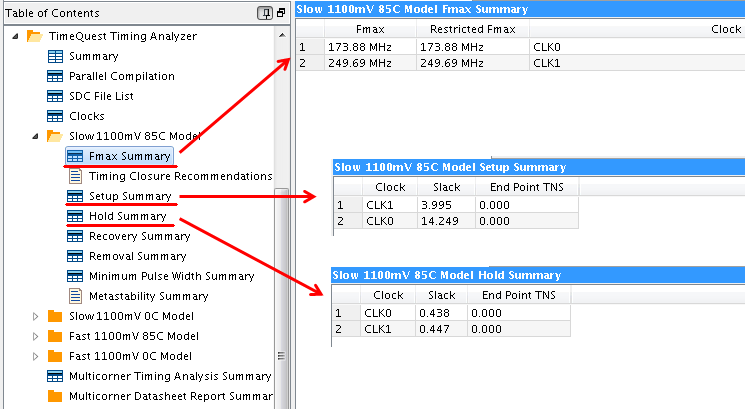
Cyclone® V GX の場合、タイミング解析に使用されるタイミング・モデルは4種類(最悪値・最高動作温度、最悪値・最低動作温度、最速値・最高動作温度、最速値・最低動作温度)あり、すべてのモデルでタイミングが希望値を満たしている必要があります。
各モデルで算出され、かつ作成した SDC の要求値と比較した結果が各フォルダに保存されています。もし要求値を満足しない項目があれば項目名が赤文字で表示されますが、すべて黒文字なので、一目で要求値をパスしたことがわかります。
もしもタイミング違反している場合には、Timing Alalyzer を使って、解析を行いながら改善に努めてください。
最後に、Beryll ボードに実際に設計してきたデザインを書き込んで、動作させてみましょう。
Beryll の FPGA でクロック同期によるLチカ![#3/3] へ続く
Beryll の FPGA でクロック同期によるLチカ!シリーズ
Beryll の FPGA でクロック同期によるLチカ![#1/3]
Beryll の FPGA でクロック同期によるLチカ![#2/3]
Beryll の FPGA でクロック同期によるLチカ![#3/3]
関連商品