- Semiconductor BusinessHOME
- Products and Services of Macnica,Inc.
-
technical information

-
Events and Seminars
- Handling Manufacturer
- Support
- Inquiry
- Click here to purchase products
- Semiconductor business e-mail magazine registration


 Narrow down by specifying conditions
現在2240件がヒットしています。check

hello.
I'm Hanako F. Altera, and I provide technical support for Altera® FPGA products at Macnica.
The design of "The first flashing light on an FPGA!" that I introduced before was a circuit that did not require a clock input signal, but this time, we will use an HDL design that operates using the oscillator (clock) mounted on the board. Make it and flash the L.
For users new to FPGA design,
Talking about clock synchronous design and global clocks, which are important for digital logic circuits, designs using clock selectors (formally, clock control blocks) available in recent FPGAs such as the Cyclone® V series I will tell you about it.
I'd also like to briefly touch upon the logic synthesis of the design. Regarding pin configuration, I'll explain a few FPGA features as I go along.
This is the board we'll be using for the LED blinking project! It's the Beryll from Mpression.
Beryll is an FPGA development board equipped with the Cyclone® V GX, which is positioned as a low-cost product in Altera® FPGA's lineup.
This guide uses the Beryll board and Cyclone® V FPGA, but it also includes content that can be applied to development with other Altera® FPGAs, so please use it as a reference. There's a lot to cover this time!
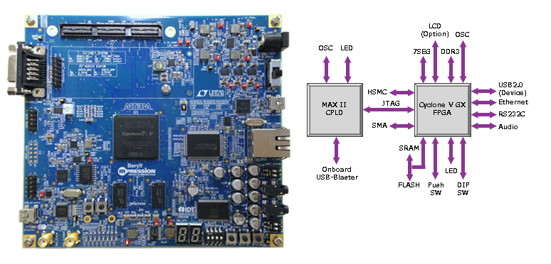
Features of Beryll
- Flexible development and verification of user logic with Cyclone® V GX FPGA
- Equipped with HSMC (High-speed Mezzanine Connector) for system expansion
- Built-in On-Board USB-Blaster™ circuitry allows you to download FPGA configuration circuitry by connecting a USB-miniUSB cable (i.e. no USB-Blaster™ required)
- HMC (Hard Memory Controller) on Cyclone® V FPGA can be evaluated with Micron's DDR3 SDRAM
For more information on Beryll, please click here.
Things necessary
- Quartus® Prime Lite Edition (the paid Standard Edition is also acceptable)
- USB-miniUSB cable, power adapter (included with Beryll board)
FPGA/Clock/Pushbutton/LED on the board and design configuration looks like this
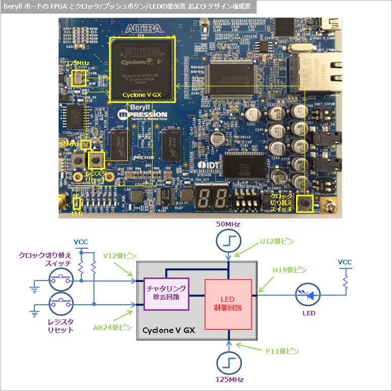
The LED blinking design specification this time uses the clock input from the outside to move the flip-flop inside the FPGA and blink the LED.
Beryll's FPGA is supplied with oscillators with different frequencies (27MHz / 33MHz / 50MHz / 125MHz), and this demo uses two of these clocks.
Design a flip-flop that operates while switching the clock supplied to the FPGA with a push button. (In other words, the flashing speed changes depending on whether the push button is ON or OFF.
The design of "The first LED blinking in FPGA!" didn't care about chattering to the push button.
I skipped the lecture because I focused on the fact that even if the LED ON/OFF is chattering, it is not visible to the naked eye, and that the contents of the design flow of Quartus® Prime for novice users of FPGA design were emphasized.
…But! But it's actually very important. There are various ways to remove chattering, and there is no set rule.
There is also a method of mounting a circuit that eliminates chattering on the board before inputting the signal to the FPGA, but this time we will design a logic circuit that eliminates chattering and implement it inside the FPGA.

What is chattering?
This is a phenomenon in which the contact of a toggle switch or push-button switch bounces immediately after it is turned ON/OFF, repeating ON/OFF several times in a short period of time before turning ON or OFF (contact state).
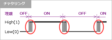
The chattering time varies from several ms to several tens of ms depending on the switch, but it is long enough for FPGAs that operate in units of several ns. To do. In other words, it appears that the switch has been operated multiple times even though it should have been operated only once, causing unintended behavior.

In this design, the transition period of the High/Low output from the FPGA must be lowered in order to blink the LED at a speed that can be seen by humans instead of observing the L blinking operation with a logic analyzer or oscilloscope. .
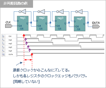
One might think that simply lowering the clock frequency could be achieved by repeatedly dividing the output of one flip-flop and reusing it as the clock for the next flip-flop, and then dividing that flip-flop again. However, this would mean that each flip-flop would operate on a different clock edge, leading to inconsistencies in the FPGA's internal operation. This is what is known as asynchronous design. In asynchronous design, the propagation delay of the flip-flops accumulates, and the impact of the delay becomes more pronounced in later stages of the circuit. As a result, not only is the internal operation of the FPGA affected, but the timing of the FPGA's output signals and peripheral devices also becomes difficult, making it difficult to synchronize the system on or between boards.
The fundamental principle of FPGA design is "clock-synchronous design." This is not unique to Altera® FPGAs; it is recommended by all FPGA manufacturers. Even if the circuit is designed logically, delays occur within the device due to place-and-route. Therefore, toggling internal registers in sync with the same clock edge is extremely important.
If you are a first-time FPGA logic circuit designer, please be sure to read the following page. It contains the absolute basics that are essential for designing digital logic circuits.
[Must-read for RTL design beginners] The difference between synchronous and asynchronous design
Start designing with Quartus® Prime!
Let's proceed based on the general development flow of FPGA/CPLD.
1. Design a logic circuit
Create a project and write the following logic circuit in HDL language.
- Chattering elimination circuit
- LED control circuit
- Top circuit connecting them
There are many ideas and design examples for chattering elimination circuits on the Internet, so I won't go into specific descriptions or explanations here. (Design with the clock synchronization circuit in mind.)
The LED control circuit should be a circuit that repeats High/Low (flashing) at a visible speed. Here too, all flip-flops are configured to synchronize with the clock.
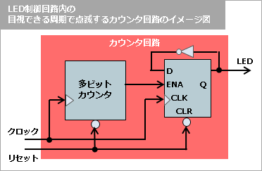
This time, the input clock to FPGA is two kinds of 50MHz and 125MHz. In order to reduce the blinking cycle to a "visible level" regardless of which clock is operated, the multi-bit counter in the image diagram is roughly configured with a 26-bit counter.
If you decide the blinking period to be "1 second", etc., calculate the number of bits of the counter and the conditions for resetting the counter from the frequency of the source vibration. This time, the same counter circuit is used for both 50MHz and 125MHz.
If you write it in VHDL language, for example, it looks like this.
| library ieee; use ieee.std_logic_1164.all; use ieee.std_logic_unsigned.all; entity Lchica_counter is port( CLK: in std_logic; ACLR: in std_logic; LEDs: outstd_logic ); end Lchica_counter; architecture rtl of Lchica_counter is signal pls_cnt : std_logic_vector (25 downto 0):=(others => '0'); signal pls : std_logic := '0'; signal led_reg : std_logic :='0'; begin process (CLK, ACLR) begin if (ACLR = '0') then pls_cnt <= (others => '0'); led_reg <= '0'; elsif (clk'event and clk = '1') then if (pls_cnt = X"2AAAAAA") then pls_cnt <= (others => '0'); pls <= '1'; else pls_cnt <= pls_cnt + '1'; pls <= '0'; end if; if (pls = '1') then led_reg <= not led_reg; end if; end if; end process; LED <= led_reg; end rtl; |
This demo is designed to switch between a 50MHz operation circuit and a 125MHz operation circuit with a push button. The logic circuit configuration is up to the user, but the circuit configuration greatly affects Quartus Prime compilation results, such as the number of logics used (consumed) in the FPGA and operating speed.
Here, we will explain the difference between two configuration examples (below) that can realize this demo.
Pattern A (left figure) is a configuration in which a counter circuit that reduces the blinking period is prepared for 25MHz and 125MHz, respectively, and selected and output at the final stage. Of course, it is a clock synchronous design.
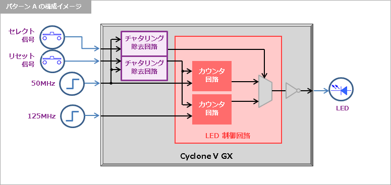
Pattern B (figure on the right) has a single counter circuit that reduces the blinking cycle, and selects the input clock in the preceding stage. Of course, this is also a clock synchronous design.
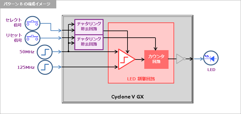
In the case of FPGA, if the clock input from outside is passed through logic such as division or selection inside, it is usually no longer a global clock.
(See here for the global clock.)

Looking at the clock configuration of this pattern B, the clock is selected, that is, it goes through a combinational circuit. Since this goes against the definition of a global clock, the flip-flops in the subsequent counter circuit are driven by clock signals other than the global clock, making it difficult to synchronize each flip-flop.
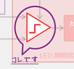
But don't worry! I'm using ALTCLKCTRL! (Right figure)
ALTCLKCTRL is a megafunction (a free vendor library. It's like an IP) that can be placed in a clock control block that can be connected to a global dedicated line. I have. By using this, even if 50MHz and 125MHz are multiplexed, the flop-flop clock in the latter stage is treated as a global clock.
ALTCLKCTRL supports Cyclone® V GX, so let's create one in Quartus® Prime's IP Catalog (Tools menu)!
Beryll's FPGA flashes by clock synchronization! Continued on [#2/3]
What is Global Clock?
The FPGA has dedicated clock lines called global clocks. This dedicated clock line is designed to have extremely small clock skew (time difference between clocks reaching all flip-flops) for the entire FPGA. By using this dedicated line as a clock, each Synchronization of flip-flops can be achieved, making timing adjustment and timing analysis easier. In addition, driving many flip-flops with a single clock consumes a lot of routing resources because the clock signal has a high fan-out. can be driven, and routing resources can be prioritized for data transfers, thus improving the overall performance of the FPGA.
You can use global dedicated lines by assigning clocks to dedicated pins determined by the device or by applying logic options to clock signals in Quartus Prime. Also, the clock output generated by the PLL (phase lock loop) is automatically connected to the global dedicated line. Any global clock signal is removed from the global dedicated line (moved to normal I/O routing) when used as an input signal to a combinational circuit or connected to anything other than the clock port of a flip-flop.
The type and number of global lines differ depending on the target device family, so please refer to the device handbook. (This is enough for today.)
Beryll's FPGA flashes by clock synchronization! series
Beryll's FPGA flashes by clock synchronization! [#1/3]
Beryll's FPGA flashes by clock synchronization! [#2/3]
Beryll's FPGA flashes by clock synchronization! [#3/3]