- Semiconductor BusinessHOME
- Products and Services of Macnica,Inc.
-
technical information

-
Events and Seminars
- Handling Manufacturer
- Support
- Inquiry
- Click here to purchase products
- Semiconductor business e-mail magazine registration
![]()
![]() Narrow down by specifying conditions
Narrow down by specifying conditions
現在2175件がヒットしています。check


hello.
My name is Intel F. Hanako and I provide technical support for Intel® FPGA products at Macnica.
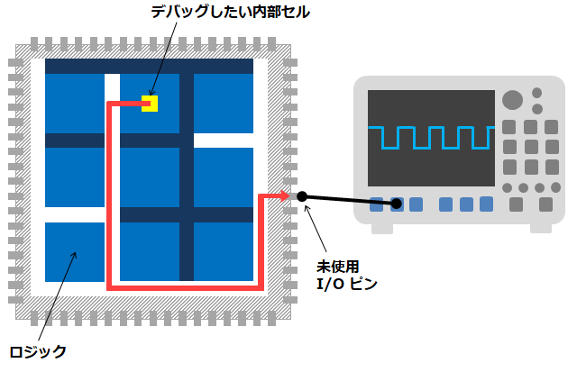
The Intel FPGA development software Quartus ® Prime has various debug features.
One of them is Signal Probe.
Signal Probe is a debugging method that outputs internal signals of the FPGA operating on the board to unused user I/O pins and observes the signals with an external device (oscilloscope, logic analyzer, etc.).
Besides!
It is possible to output (route) internal signals to pins without editing the design while preserving the results of the previous compilation.
Efficient debugging.
Features of Signal Probe
Signal Probe has the following features:
・Using an external device
- Internal signals can be routed to monitor pins without editing the design
・Consume almost no internal resources of the device
Requires spare user I/O pins for debugging
・JTAG connection not required
・Can be used free of charge
Below is a comparison of the Signal Probe and Signal Tap logic analyzers.
|
requirement |
Signal Probe |
Signal TapLogic Analyzer |
| Requires external equipment |
〇 |
× |
| Requires JTAG connection |
×(1) |
〇 |
| Adding User I/O Pins |
〇 |
×(2) |
|
unused internal logic and internal memory required |
× |
〇 |
| Advanced trigger functions |
× |
〇 |
Notes:
(1) JTAG connection is required when writing sof/pof data
(2) Consumed when using trigger inputs and outputs
Eligible Quartus Prime
Signal Probe is a feature supported by Quartus Prime below.
・Quartus Prime Pro Edition
・Quartus Prime Standard Edition
・Quartus Prime Lite Edition
Target device
Signal Probes are available for all families supported by your Quartus Prime.
* Please use Quartus Prime Pro Edition for Arria® 10. (Standard Edition is not supported.)
* CPLDs without internal memory can also be used.
Method of operation
Compilation of the user design must be completed before executing Signal Probe.
Also, the operation method differs depending on the version of Quartus Prime.
|
Quartus Prime |
Work content |
How to respond |
compile |
| Pro Edition |
・Create pins for Signal Probe
・Pins for Signal Probe Assigning internal signals to monitor
|
set by script |
Rapid Recompile |
|
Signal Probe dedicated Set by GUI |
Signal Probe Compilation (ECO * Compile) |
* ECO : Engineering Change Order
How to use Quartus Prime Pro Edition
In the Pro Edition, the following operations are set by scripts.
・ Create pins for Signal Probe
・ Allocate internal signals to be monitored to Signal Probe pins
In the example below, we will refer to the pin name for the Signal Probe as sp_moni.
It is assumed that the project design has already been compiled.
(1) Open the .qsf file of the project in text by File menu > Open.
② Add and save the following command to the .qsf file to reserve the Signal Probe pin.
<pin_name> specifies the name of the pin you created for your Signal Probe.
set_global_assignment -name CREATE_SIGNALPROBE_PIN <pin_name>
(Example) set_global_assignment -name CREATE_SIGNALPROBE_PIN sp_moni
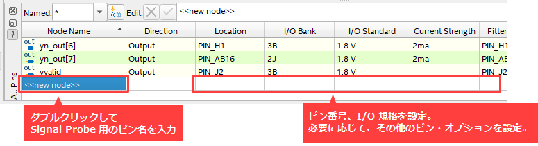
③ In Pin Planner, register the pin name created for Signal Probe in ② above in <<new node>> in the Node Name column,
Specify the pin number, I/O standard, etc.
④ Execute compilation.
⑤ Add and save the following commands to the .qsf file and assign internal nodes to the pins created for the Signal Probe.
set_instance_assignment -name CONNECT_SIGNALPROBE_PIN <pin_name> -to <node_name>
<pin_name> specifies the name of the pin you created for your Signal Probe.
<node_name> specifies the internal node you want to monitor.
Since internal nodes must be described with a hierarchical path, in View menu > Node Finder
Set the Filter to "Signal Tap: post-fitting" and use the node name found by the Search button.
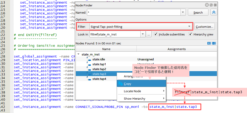
Copy the desired node name and paste it in the <node_name> part. At that time, the top-level entity name is unnecessary, so please delete it.
(Example) set_instance_assignment -name CONNECT_SIGNALPROBE_PIN sp_moni -to state_m_inst|state.tap3
⑥ Recompile the design.
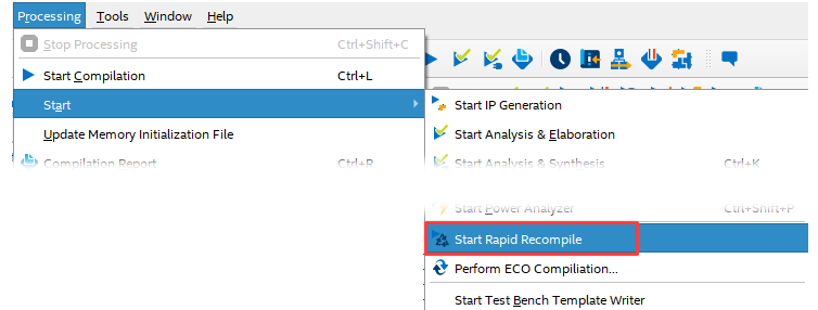
At this time, if you only add Signal Probe pins without changing the design, instead of the usual full compilation
Running Rapid Recompile is recommended!
Processing menu > Start > Start Rapid Recompile
To run Rapid Recompile in Pro Edition, a snapshot must be generated in the Fitter.
To generate Fitter snapshots, a full compilation must be performed with the following options enabled:
Enable Intermediate Fitter Snapshots = On (in Assignments menu > Settings > Compiler Settings)
* This option does not exist in ver.18.0 Pro Edition.
(When running Rapid Recompile, the message "Rapid Recompile database does not exite."
If you don't get the error "Rapid Recompile could not locate a design database from a previous compilation on disk."
Not required. )
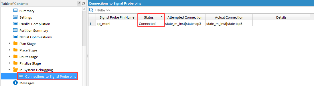
⑦ In the compilation report (Processing menu > Compilation Report),
Click Fitter folder > In-System Debugging folder > Connections to Signal Probe pins
Check the Status column notation to see if the internal signal was routed to the Signal Probe pin.
|
Status |
explanation |
| Connected | Routing successful. |
| Unconnected |
Routing was not successful. Possible reasons are: • Not routable because the node belongs to an I/O cell or another hard IP. • The node hierarchy path does not exist in the design. ・The node is not Signal Tap: post-fitting. |
⑧ After writing the file to the device, observe the pin with the Signal Probe set using an external measuring instrument (logic analyzer, oscilloscope, etc.).
That's all for Signal Probe operation in Pro Edition.
Operation by Quartus Prime Standard/Lite Edition
In the Standard and Lite Editions, the following operations are set using the Signal Probe dedicated GUI.
・ Create pins for Signal Probe
・ Allocate internal signals to be monitored to Signal Probe pins
In the example below, we will refer to the pin name for the Signal Probe as sp_moni.
It is assumed that the project design has already been compiled.
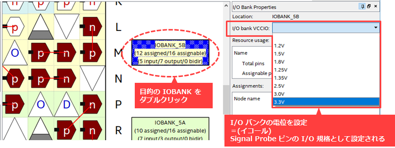
(1) Set the I/O standard in advance for the pins for Signal Probe.
Note:
The I/O standard of the pins for Signal Probe depends on the VCCIO potential setting value of the I/O bank to which the pin number to be placed belongs.
If you have not set the VCCIO voltage for the I/O bank uniquely, set it with Voltage in Device and Pin Options (Assignments menu > Device).
It depends on the potential setting value of Default I/O Standard.
Therefore, set in advance the potential of the I/O bank to which the pin number assigned to the Signal Probe pin belongs.
[Reference information] What is an I/O bank? (See "What is an I/O bank?" on the linked page.)
Launch Assignments menu > Pin Planner and double-click the desired IOBANK_XX.
In the I/O Bank Properties window that appears, set the I/O bank VCCIO.
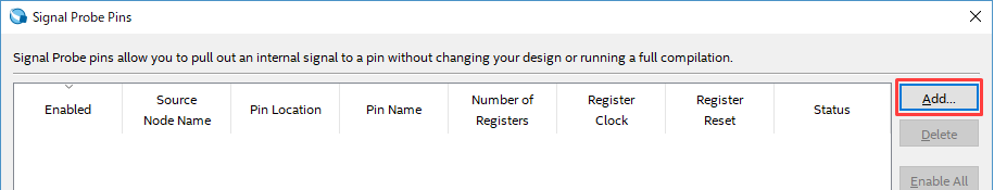
(2) Start Tools menu > Signal Probe Pins.
Click the Add button to display the Add Signal Probe Pin dialog Box.
③ Click the browse button to the right of Source node name in the Add Signal Probe Pin dialog Box to start Node Finder.
Set Filter to "SignalProbe" and click the List button.
From the discovered nodes, select the nodes to monitor from the Matching Nodes column to the Nodes Found column.
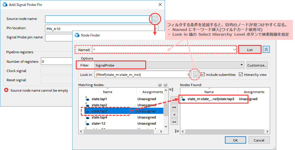
④ Set other items in the Add Signal Probe Pin dialog Box.
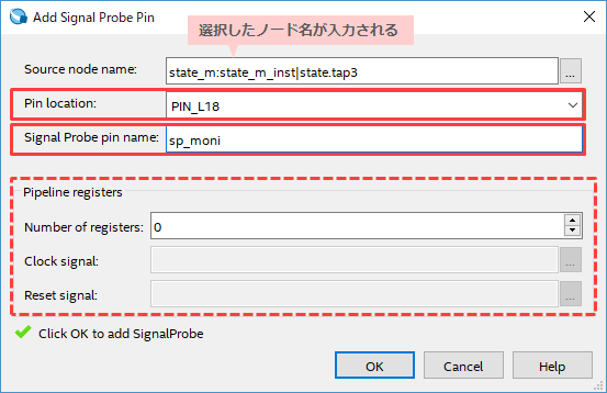
| Pin location |
Select a pin number to assign a pin for Signal Probe. (Only unused user I/O pin numbers are shown in the list) |
| Signal Probe pin name |
Enter the pin name for Signal Probe. (for this example, type sp_moni) |
| Pipeline registers |
If you want to insert a register into the signal output by Signal Probe, set the following: - Number of registers to insert ・Clock signal that controls registers ・Reset signal that controls registers |
To change the contents after setting, double-click each item and edit.
⑤ Execute Signal Probe Compilation.
Processing Menu > Start > Start Signal Probe Compilation
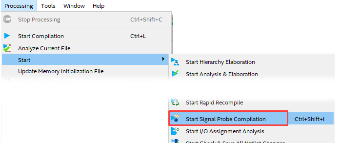
ECO (Engineering Change Order) compilation is performed.
If Start Signal Probe Compilation is inactive and cannot be selected, launch Tools menu > Signal Probe Pin and
Click the Start Check & Save All Netlist Changes button at the bottom right of the dialog Box.
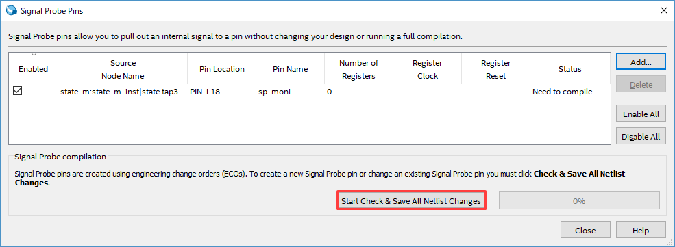
After confirming the message “ECO Fitting was successful”, Signal Probe Compile is completed.
Hanako's point♪
If the following error occurs during Signal Probe Compilation, the I/O standard of Signal Probe Pin may not be set correctly.
ID:169026
Pin <name> with I/O standard assignment <name> is incompatible with I/O bank <name>. I/O standard <name>, has a VCCIO requirement of <number>, which incompatible with the I/O bank's VCCIO setting or with other output or bidirectional pins in the I/O bank using a VCCIO requirement of <number>. pin to a compatible I/O standard. The Intel FPGA Knowledge Database contains many articles with specific details on how to resolve this error. Visit the Knowledge Database at https://www.altera.com/support/support-resources/knowledge- base/search.html and search for this specific error message number.
See here for a workaround.
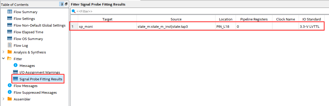
⑥ In the compilation report (Processing menu > Compilation Report),
Click the Fitter folder > Signal Probe Fitting Results to see if the internal signals were routed to the Signal Probe pins.
⑦ After writing the file to the device, observe the pin with the Signal Probe set using an external measuring instrument (logic analyzer, oscilloscope, etc.).
That's all for Signal Probe operation in Standard and Lite Editions.
How to avoid Error ID: 169026 in Signal Probe Compilation
(* Standard and Lite Edition only)
The cause of Error ID: 169026 during Signal Probe Compilation is
This is because the potential of the I/O standard set on the Signal Probe pin does not match the VCCIO potential of the I/O bank to which the Signal Probe belongs.
As a workaround, do the following:
- In Signal Probe Pins, delete the corresponding setting (Delete)
- Correctly set the potential of the I/O bank as in step 1.
- Set the pins again in Signal Probe Pins
- Execute Start Check & Save All Netlist Changes in Signal Probe Pins
Click here for recommended articles/materials
Try FPGA on-chip debugging "Signal Tap"
Quartus® Getting Started Guide - Using the Signal Tap Logic Analyzer
Intel® FPGA Development Flow/FPGA Top Page