
![]()
![]() Narrow down by specifying conditions
Narrow down by specifying conditions
現在1888件がヒットしています。check

When creating a board to implement an Intel® FPGA, the designer creates a schematic by referring to the documentation published by the manufacturer.
Here, we will guide you to the points that you should pay special attention to.
It should be noted that Q
Target FPGA
・ Intel® Arria® 10 FPGA
Advance preparation
Here are some documents that can be used as reference when creating circuit diagrams.
|
Pin connection guidelines |
Schematic review worksheet |
| Arria 10 Device Family Pin Connection Guidelines | Arria 10 Devices Schematic Review Worksheet |
Arria 10 Overview (FPGA TOP)
The figure below shows the pins that need special attention in the Arria 10 board design.
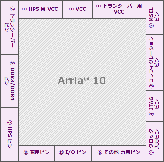
* The layout in the diagram has nothing to do with the actual device.
Click each item to see the check points.
① VCC, VCC for HPS, VCC for transceiver
|
● Establish a measurement point near the FPGA ・Be ready to measure the power supply in case of trouble |
|
● If all transceivers, fPLLs, and IOPLLs on the same side are unused, ・VCCR_GXB and VCCT_GXB can be connected to GND ・VCCH_GXBR can be connected to GND (Check pin connection guidelines for details) |
|
● Decoupling capacitor ・Estimate with reference to the PDN tool ・For a more detailed estimate, use a dedicated tool <Reference> Power Delivery Network (PDN) Analysis Tool Part 9 Confirmation and Review of Capacity in FPGA Power Supply Design |
|
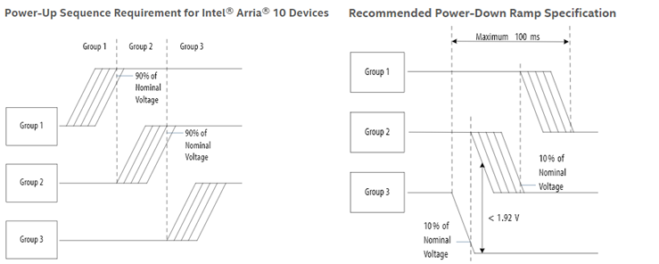
● Power sequence See this document (Power Sequencing Considerations for Intel Arria 10 Devices) for more details. |
② MSEL pin
Please see below for Arria 10 MSEL pin information.
|
MSEL Pin Settings |
Inserting pull-up/pull-down resistors(1)(2) |
|
* Refer to "MSEL Pin Settings" on the link |
(see linked documentation) |
(1) A Weak Pull-Down Resistor (25kΩ) is inserted inside.
(2) If you want to switch the configuration mode, insert a 0Ω resistor to switch to VCCPGM/GND.
(3) Do not drive the MSEL pins with a microprocessor or other device.
(4) Use PS or FPP MSEL pin settings for configuration via HPS.
See here for a list of MSEL pins.
③ Configuration pin
|
● DCLK ・Recommend inserting damping resistor (minimum 0Ω) 10-50Ω ・In AS mode, take care of the trace length (see the document below) Trace Length Guideline (from "Configuration, Design Security, and Remote System Upgrades in Intel Arria 10 Devices") |
|
● nCONFIG, nSTATUS ・Pull up to VCCPGM via 10kΩ resistor |
|
● CONF_DONE ・Pull up to VCCPGM via 10kΩ resistor ・Do not connect to the LED as it is. - Due to lack of drive current, it may not light up without applying FET |
|
● CLKUSR ・When using a transceiver or HMC (Hybrid Memory Cube) - use CLKUSR as their calibration clock (required) - must be entered before configuration - For AS mode, input 100MHz clock - For PS, FPP mode, input 100 ~ 125MHz clock |
|
● Refer to AN822: Intel FPGA Configuration Device Migration Guideline for migration from EPCS/EPCQ to EPCQ-A |
|
● When FPGAs are cascaded, nSTATUS and CONF_DONE are pulled up in common. |
|
● nCE ・Connect to GND for single device configuration. ・This signal determines whether the FPGA is cascaded. |
|
● When using nCEO, pull up to VCCPGM through a 10kΩ resistor. |
④ JTAG pins
|
● Check Point ・It is recommended to insert a 0Ω damping resistor for TCK. - To support cases where writing is not possible due to problems with the clock system |
|
● Pin processing ・TCK: pull down via 1kΩ resistor ・TDI: Pulled up to VCCPGM via 1kΩ to 10kΩ resistor ・TMS: Pulled up to VCCPGM via 1kΩ to 10kΩ resistor ・TDO : No pull-up/pull-down ・TRST : Option used. Pull up to VCCPGM through a 1 kΩ resistor if unused. |
| ● When cascading three or more FPGAs, insert buffers on the TCK and TMS lines. |
⑤ Clock input pin
|
● When using a single-ended clock, assign it to the p-channel (Does not ride on global clock directly on n-channel. Limitation when using ALTCLKCTRL buffer) |
|
● Connect clock input pins that are not shared with I/O pins to GND if they are not used. |
|
● Pay attention to AC/DC coupling when inputting differentially. |
|
● If you are using a PLL, pull down the RREF pin through a 2kΩ resistor (resistor accuracy is ±1%). |
|
● CLK and PLL pins can be left unconnected if not used. |
* See "Clock and PLL Pins" in Arria 10 Device Family Pin Connection Guidelines for clock input pin names
⑥ Other dedicated pins
|
pin name |
comment |
| RREF_[T,B][L,R] |
Pulled down through a 2kΩ±1% resistor |
| VREFB* | Tie to VCCIO or GND in the same bank if not used as a dedicated pin |
| VREFP_ADC / VREFN_ADC | Connect to GND if not used as a dedicated pin. |
|
TEMPDIODEp/n |
Connect to GND if not used as a dedicated pin. |
⑦ Transceiver Pins
|
● When not using the transceiver ・Clocks (REFCLK_GXB*_CHp/n) are individually connected to GND or collectively pulled down via a 10kΩ resistor. ・RX (GXB*_RX_*p/n) is connected to GND ・TX (GXB*_TX_CHp/n) is floating |
|
● AC/DC coupling ・Adjust to I/O Standard |
⑧ DDR3/DDR4 pin
Please refer to the following web content and check according to the guidelines.
⑨ HPS pin
|
Cyclone V SoC Pin Names |
comment |
|
BOOTSEL[2:0] |
Pulled up or down to VCCIO voltage through a 4.7kΩ resistor |
|
HPS_nRST (bidirectional pin) |
Pulled up to VCCIO_HPS voltage through a 1kΩ resistor |
|
SDMMC |
Pulled up through a 10kΩ resistor |
⑩ Dual-purpose pin
|
● Connect to GND if not used as a function pin and not used as a user I/O pin. ・ CLKUSR ・ DEV_OE ・DEV_CLRn ・PR_REQUEST |
| ● If nPERST is used as a reset pin for PCIe hard IP, shift down the voltage from 3.3V LVTTL to 1.8V and connect it through a level translator. |
⑪ I/O pins
RZQ pin handling is required for internal calibration.
Recommended to use the RZQ pin to enable the internal calibration feature.
If using 2.5/3.0-V, check if the device supports it.
Appendix: Arria 10 MSEL Pin Table
MSEL Pin Settings (FPGA Configuration)
|
Device Family |
Configuration Mode |
VCCPGM(V) |
POR Delay |
MSEL[2:0] |
|
Arria 10 |
AS (x1, x4) |
1.8 |
Fast |
010 |
| Standard |
011 |
|||
|
PS, FPP (x8, x16, x32) |
1.2/1.5/1.8 |
Fast |
000 |
|
| Standard |
001 |
MSEL Pin Settings (HPS Configuration)
|
Device Family |
Configuration Mode |
VCCPGM(V) |
POR Delay |
MSEL[2:0] |
|
Arria 10 SoCs |
FPP (x16, x32) |
1.8 |
Fast |
000 |
| Standard |
001 |
Click here for recommended articles/materials
FPGA Power & Thermal Design & Debug Guidelines
Active Serial Configuration Design & Debug Guidelines