- Semiconductor BusinessHOME
- Products and Services of Macnica,Inc.
-
technical information

-
Events and Seminars
- Handling Manufacturer
- Support
- Inquiry
- Click here to purchase products
- Semiconductor business e-mail magazine registration
![]()
![]() Narrow down by specifying conditions
Narrow down by specifying conditions
現在2183件がヒットしています。check
The cross-sectional dimension of the port is an important factor that determines the cost, but I often see cases where it is left up to the board maker, or where it is decided for some reason.
We've talked about cross-sectional dimensions several times.
See also
- How to determine the cross-sectional dimensions of the board
- Cross-sectional dimensions of the substrate surface layer - Part 1
- Cross-sectional dimensions of the substrate surface layer - Part 2
- Board differential transmission pattern design
- Cross-sectional dimensions of the intermediate layer of the substrate
This time, in two parts, I will examine the approximation formulas that determine the board parameters that are often used, and on the contrary, I will introduce two tools that determine the cross-sectional dimensions from the specifications.
I will introduce this tool next time, but I will give only the tool to those who want it. Please see the end of the sentence.
Required specifications
The required specifications (substrate parameters) for determining the cross-sectional dimensions of the board are
(a) Characteristic impedance Z0
(b) Wiring density W and G
(c) crosstalk coefficient ξ
Etc.
The characteristic impedance Z0 of (a) is usually chosen to be 50Ω.
The reason is,
- Easy to make, if you make it normally, it will be around 50Ω
- I want to match with others when connecting multiple boards
- Somehow sharp
I guess.
I think that the 50Ω of the measuring instrument is irrelevant except for special applications.
However, the actual situation is that it is 50Ω without thinking about why it is 50Ω. But there's nothing wrong with that.
In the TTL era before CMOS, characteristic impedance of 80Ω or 100Ω was convenient for waveform transmission due to the characteristics of the driver.
Trivia "Optimum Z0 for TTL is 100Ω Please refer to
In today's CMOS, the output impedance (on-resistance) can be easily selected arbitrarily by changing the transistor size, so there is no need to select the characteristic impedance of the board according to the characteristics of the driver as was the case in the TTL era. Rather, it is important to design a driver that matches 50Ω, which is easy to make. Unfortunately, due to a lack of awareness among driver manufacturers, the driver is not designed that way, so the actual on-resistance value is much smaller than the optimum value (driving capability is large). Therefore, a damping resistor is required to reduce waveform disturbance when Z0=50Ω. This is a little disappointing.
Damping resistors have been mentioned several times.
See below.
- How to decide the value of damping resistor?
- where to put the damping resistor
- Damping resistor value to be determined more easily
- Freshers: Damping Resistance - Part 1
- Freshers: Damping Resistance ~ Part 2
For (b), it is required from the viewpoint of cost to increase the mounting density by selecting the pattern width W as small as possible and the gap G between patterns as narrow as possible within the range of yield.
This is quite obvious, but unfortunately we see many examples that are made carelessly and are not given much thought.
(c) conflicts with the selection of the inter-pattern gap G in (b), but G is determined from the crosstalk requirements. Choosing a large G reduces crosstalk.
I think that it should be decided from the noise budget rather than just deciding.
Analysis software (solver)
A special tool is used to obtain the electrical specifications from the cross-sectional dimensions.
The author
Green Express V2
Green Express Professional
Unfortunately, these products have been discontinued and are no longer available.
There are other products from Polar Instruments, but they are a little more expensive.
It seems that some are attached to the circuit analysis software.
I'm sure there are others, but I haven't researched them much.
microstrip line = surface layer
Several approximations have been proposed for ease of determination.
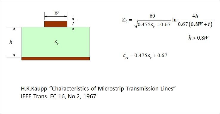
A famous one is Kaupp's 1967 paper, shown in Figure 1.
However, since it is half a century old, the dimensions of the board are far from the current specifications. There are some assumptions, but I feel that this approximation formula is going it alone without considering them properly.
The following is an explanation based on the contents of this paper, but I do not criticize this paper, but pay tribute to the fact that the approximations of the materials and dimensions of the time have been used for half a century. However, now that the dimensional conditions are different from those days, it will be necessary to review it properly.
equivalent dielectric constant
εre in Figure 1 is the equivalent dielectric constant of the microstrip line.
This formula does not include pattern width W, thickness t, and distance from ground (height) h.
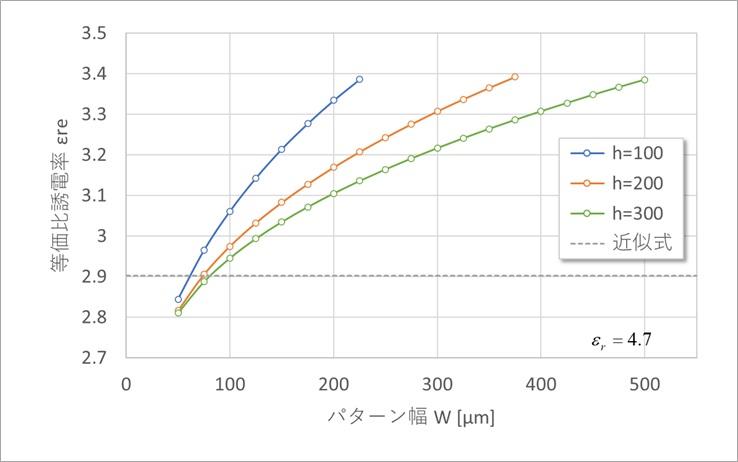
Fig. 2 shows the equivalent relative permittivity obtained by calculation when these are changed. When εr = 4.7, Kaupp's approximation gives εre = 2.9, but it varies from 2.8 to 3.4 depending on W and h.
The square root of εre affects the delay time. It works with the square root, so it's a few percent error, but you need to be aware of it.
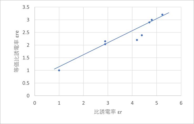
Figure 3 shows the plot and approximate straight line when obtaining the equivalent relative permittivity described in Kaupp's paper. Linear approximation is performed for samples with dielectric constants of 1 to 5.2. Since the dielectric constant used in actual printed wiring boards is about 4 to 5, it deviates considerably from the approximation formula in this range.
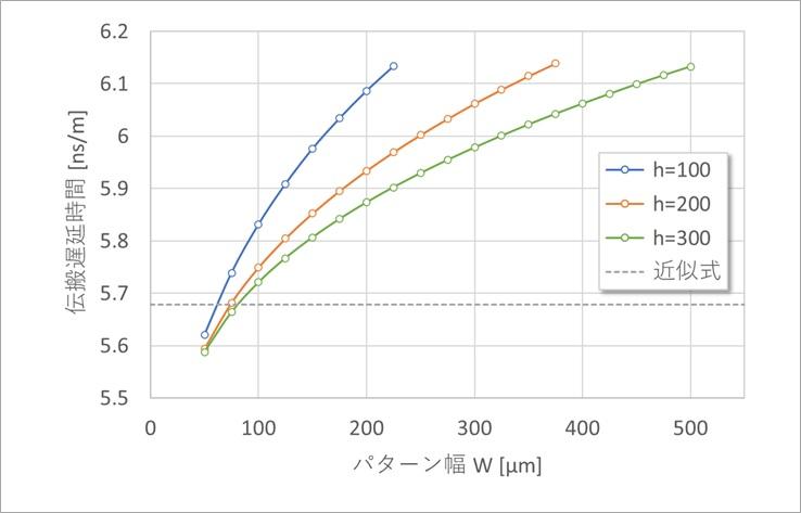
Figure 4 also shows the propagation delay time. It ranges from 5.6ns/m to 6.1ns/m with a width of about 10%.
Be careful when you need exact values.
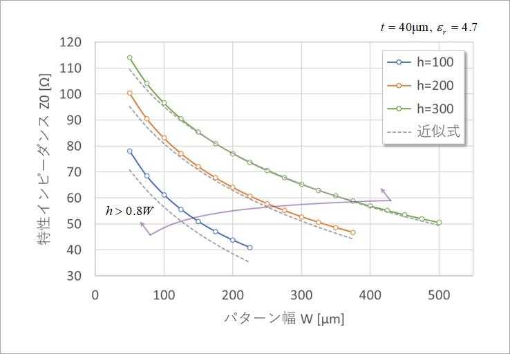
Figure 5 plots the approximation of Figure 1. There is a condition of h>0.8W, but it seems that this condition is not very necessary. More than that, the error increases as the distance (height) h from the ground decreases.
At the time of the publication of the paper, I think that substrates with h=100 μm were not generally put into practical use.
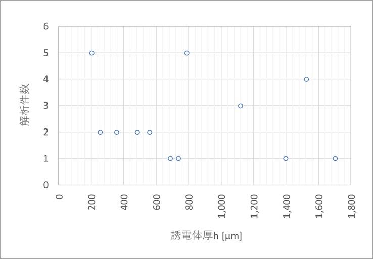
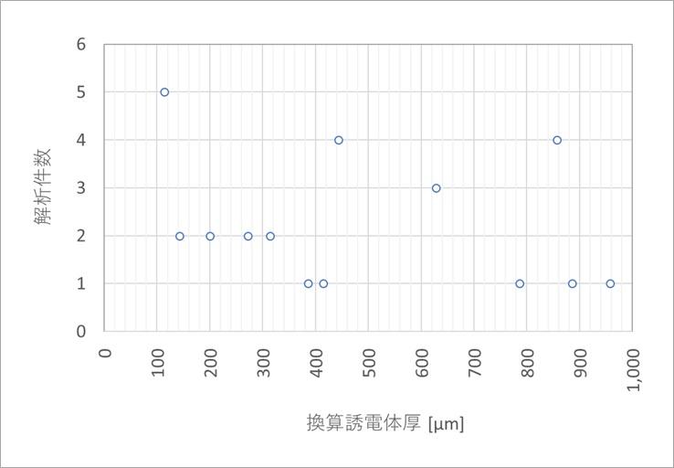
Figure 6 plots the distribution of the dielectric thickness h of the sample when comparing the calculated values with the measured data. This data shows that the conductor thickness t is about 70 μm (2.8 mil), which is thicker than the conductor thickness currently used. Notice that out of 29 samples, there are only 11 samples with a dielectric thickness of 300 μm or less. The environment has changed so much since then.
Here, let's check the cross section of the microstrip line again.
Kaupp's approximation was of the form in Fig. 1.
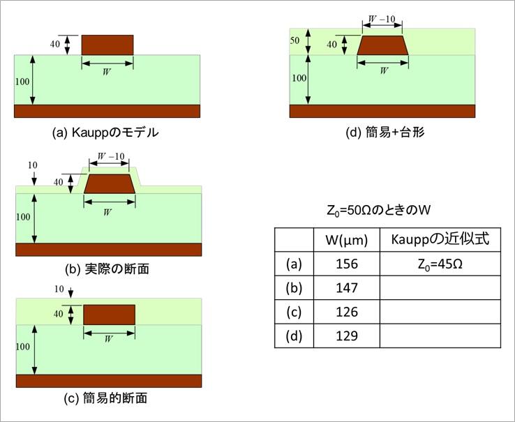
Figure 8 shows the cross-sectional shape of the microstrip line actually used in the calculation.
(a) is the shape of Kaupp's approximation formula, which is a very ordinary shape that is often used in addition to this approximation formula.
(b) is an almost accurate representation, the pattern is an upward trapezoid, and the solder mask is smoothly covered. However, it is somewhat cumbersome to analyze.
(c) is often used in approximate calculations along with (a). It does not take much time to enter analysis data.
(d) is an improved version of (c), taking into consideration the etching effect of the pattern.
The table in the same figure shows the dimensions obtained by analysis when the characteristic impedance Z0 is 50Ω for each shape. Both contain an error of about 10% to 15% for 147 μm in (b).
In practice, board manufacturers compare design values with actual measurement data and make corrections, so these errors are not a big problem.
So far, we have discussed microstrip lines.
In the next installment, I plan to make a similar consideration for striplines and introduce a tool created by the author to obtain cross-sectional dimensions for required substrate parameters.
*This tool is still in beta version and has not been released to the public.
[Message from the author]
![[Message from the author]](/business/semiconductor/articles/Kiso_Picture9.jpg)
What is Yuzo Usui's Specialist Column?
It is a series of columns that start from the basics, include themes that you can't hear anymore, themes for beginners, and also a slightly advanced level, all will be described in as easy-to-understand terms as possible.
Maybe there are other themes that interest you!