- 半導体事業HOME
- マクニカの製品・サービス
-
技術情報

-
イベント・セミナー
- 取扱メーカー
- サポート
- お問い合わせ
- 製品購入はこちら
- 半導体事業のメルマガ登録
![]()
![]() 条件を指定して絞り込む
条件を指定して絞り込む
現在2183件がヒットしています。check
現在は、ほとんどのデバイスはCMOSですが、高速のCMOSが現れる前は、ほとんどのデバイスはTTLでした。
その当時、CMOSはありましたが、例えば、メタル・ゲートのCMOS4000シリーズのように、非常に低速のため、低電力の要求が強い場合のみ使用されていました。
図1にTTL(7400)の出力の静特性を示します。
Low側(Pull Down)と、High側(Pull Up)とが非対称で、駆動能力という概念も現在とは異なっていました。
Low側は、ある電流までは出力抵抗が小さく、High側は、ほぼ100Ω程度です。
したがって、現在のCMOSで多用されている、ダンピング抵抗を挿入することは無意味でしたし、その概念もありませんでした。
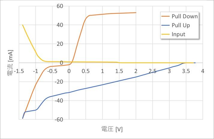
図2は、現在のCMOSの静特性とBergeron解析結果を示します。
LowとHighとがほぼ対称で、いずれも直線とみなせます。
24mAドライバに22Ωのダンピング抵抗を挿入して、ほぼきれいな応答を示しています。
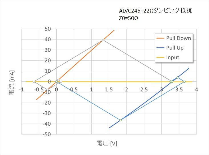
図3は、Z0=50Ωの場合のTTLのBergeron解析で、図4はその時間応答です。
横軸は、線路の片道の伝搬遅延τで正規化しています。
LowからHighの立ち上がりは、2.3V付近に最初の段が付き、その後ゆっくりと最終値に近づきます。HighからLowは、負のオーバシュートが存在しますが、一度で立ち下がります。
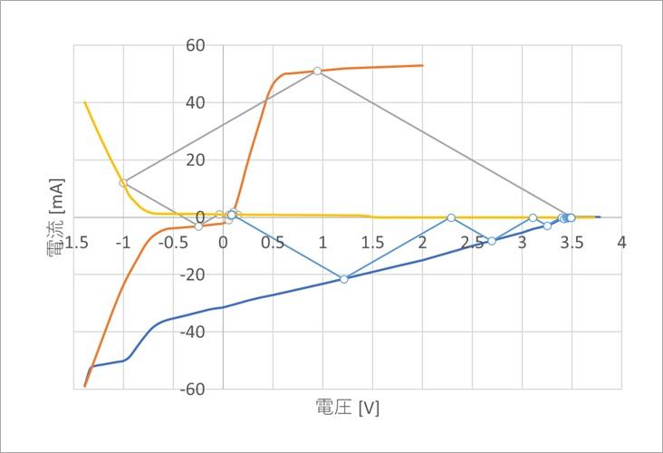
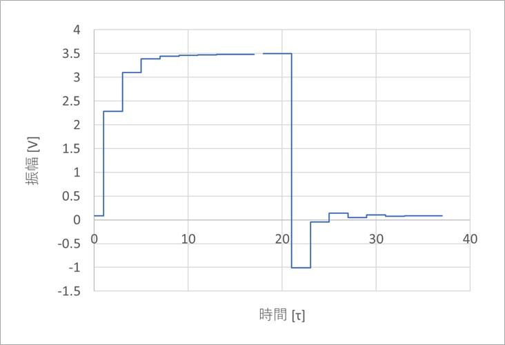
図5と図6は、同じくZ0=80Ωの場合です。
立ち上がりにやや段が付きますが、50Ωよりも良好です。
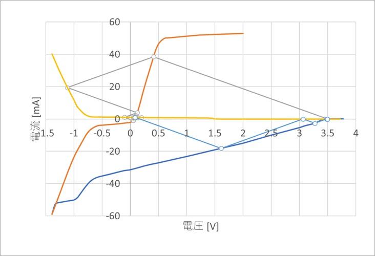
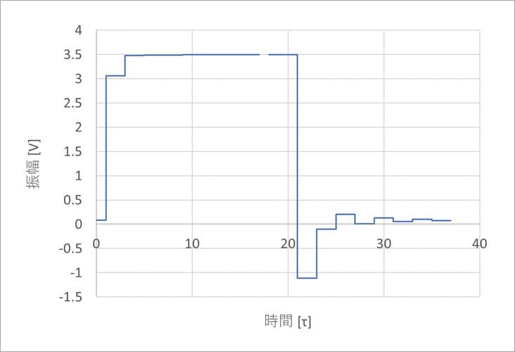
図7と図8は、同じくZ0=100Ωの場合です。
ようやく、一度で立ち上がるようになりました。

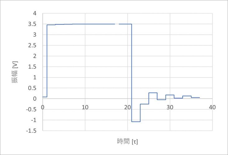
図9と図10は、同じくZ0=120Ωの場合です。
Z0=120Ωのボードは、作りにくいということと、図10に示すように、立ち上がりの最初の振幅が、Z0≦100Ωの場合の最終値よりも高くなり、High側の出力回路のエミッタホロアの特性により、定常値に落ち着くのに時間を要します。図10のLow→Highの最後の振幅と、High→Lowの最初の振幅とに差があることが分かります。
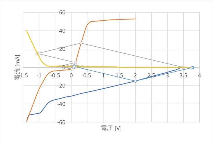
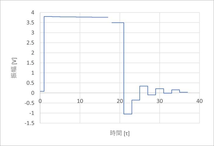
図11に、図10の立ち上がり波形を、135τまで解析した結果を示します。最初に3.7V付近まで立ち上がり、その後は、上述のエミッタホロアのベース-エミッタの逆バイアスによって、高インピーダンスとなり、じわじわと最終値の3.5Vに漸近します。
出力特性は、データシートからプロットして得たもので、実際の回路のデータとは少し異なるかもしれませんが、TTLのときにはこのような厄介な現象も考える必要がありました。定常値まで到達する前に、立ち下がると、Lowレベルがそれだけ持ち上がります。TTLは、特にLow側のマージンが少なかったので、気をつける必要がありました。
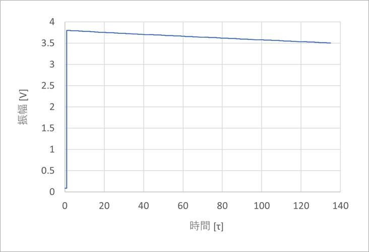
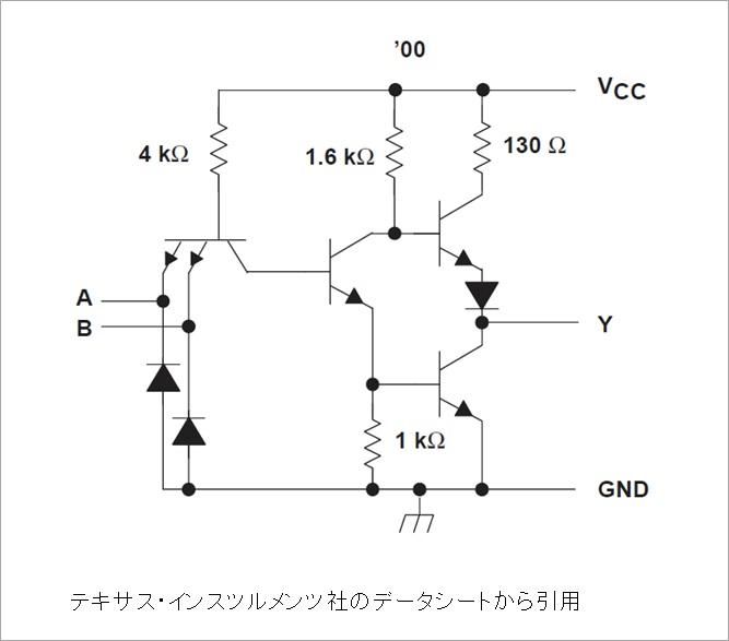
図12に、参考のために、TTLの回路図を示します。なぜ図11のような現象が生じるのか考えてください。
碓井有三のスペシャリストコラムとは?
基礎の基礎といったレベルから入って、いまさら聞けないようなテーマや初心者向けのテーマ、さらには少し高級なレベルまでを含め、できる限り分かりやすく噛み砕いて述べている連載コラムです。
もしかしたら、他にも気になるテーマがあるかも知れませんよ!