- Semiconductor BusinessHOME
- Products and Services of Macnica,Inc.
-
technical information

-
Events and Seminars
- Handling Manufacturer
- Support
- Inquiry
- Click here to purchase products
- Semiconductor business e-mail magazine registration
![]()
![]() Narrow down by specifying conditions
Narrow down by specifying conditions
現在2183件がヒットしています。check

In "Cross-sectional dimensions of the substrate surface layer - Part 1", we talked about general single transmission. This time, we will discuss differential transmission and how to further increase mounting density. (See also "Pattern Design for Differential Transmission on Board".)
differential transmission
Consider the cross section of the differential line in Figure 1. In addition, the distance between lines is represented by G (Gap) for single transmission, and S (Space) for differential signals, but please note that this is not particularly generalized and is just my personal preference. .
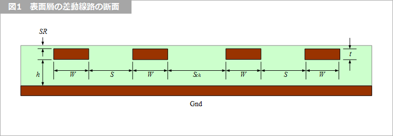
(1) Target value
As an example, consider Z0 = 50Ω, Zdiff = 85Ω, ξ23 = 0.1. ξ23 is the crosstalk coefficient between adjacent traces of two pairs of paired lines. Z0 ≒ √(ZC × ZD), Zdiff = 2 × ZD, Zcom = ZC ÷ 2, so Z0 = 50 Ω, Zdiff = 85 Ω, ZD = 42.5, ZC = Z0^2 ÷ ZD = 58.8, Zcom = 29.4.
(ξ: Greek lowercase letter Qsai)
(2) Minimum pattern width W and distance h from GND
Considering the same as single transmission, let W = 100 um and h = 100 um. At this time, Z0 = 54.7 Ω. We think that it can be regarded as approximately 50 Ω. Z0 = 50 ohms W = 126 um if you want a snug fit.
(3) Intra-pair spacing S
When S = 118 um for two lines, Zdiff = 85 Ω. When W = 126 um, S = 161 um and Zdiff = 85 Ω.
(4) Spacing between channels Sch
When Sch = 221 um for two lines, the crosstalk coefficient ξ = 0.1. For W = 126 um, Sch = 214 um gives a crosstalk coefficient ξ = 0.1.
When arranged, it looks like Table 1.
| term | Z0 | W | S | Sch | 4W+2S+2Sch |
| 1 | 54.7Ω | 100 | 118 | 221 | 1,078 |
| 2 | 50Ω | 126 | 161 | 214 | 1,254 |
The first term starts from a pattern width W = 100 um, and the second term starts from Z0 = 50 Ω. It is better to adjust Zdiff to the requested value as much as possible, but I think that Z0 is fine as long as it is close to the requested value. The width occupied by the two pairs of differential signals is 4W + 2S + 2Sch, so the dimensions are determined so that this is as small as possible.
For higher density
Since it is necessary to pass wiring between mounted parts on the surface layer, and especially between multi-pin ICs such as BGA, there is a demand to make the pattern width as thin as possible.
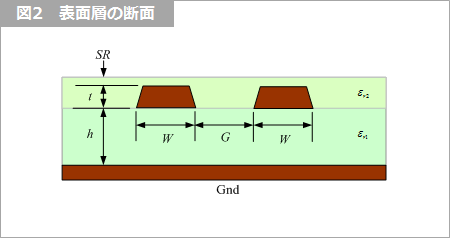
On the other hand, the pattern width considering the cost is usually about 0.1 mm, as mentioned in "How to determine the cross-sectional dimensions of the board" and "Cross-sectional dimensions of the surface layer of the board - Part 1". If it is thinner than usual, the pattern may be cut off during etching. When forming a pattern, as shown in Figure 2, the parts not covered by the resist are etched away, leaving the pattern under the resist. The result of the etch is therefore a generally trapezoidal cross-section, as shown. If the copper foil is extremely thin, the etching will be completed in a short period of time, and the degree of trapezoidal shape will be less, and a narrower pattern can be achieved.
Plating is formed on the surface copper foil in order to apply through-hole plating to the surface layer. For example, an ultra-thin surface layer can be achieved by performing "selective plating" in which plating is applied only to the holes in the through-hole plating process, or by scraping off the plating by polishing or etching. Figure 3 is an image diagram of it.
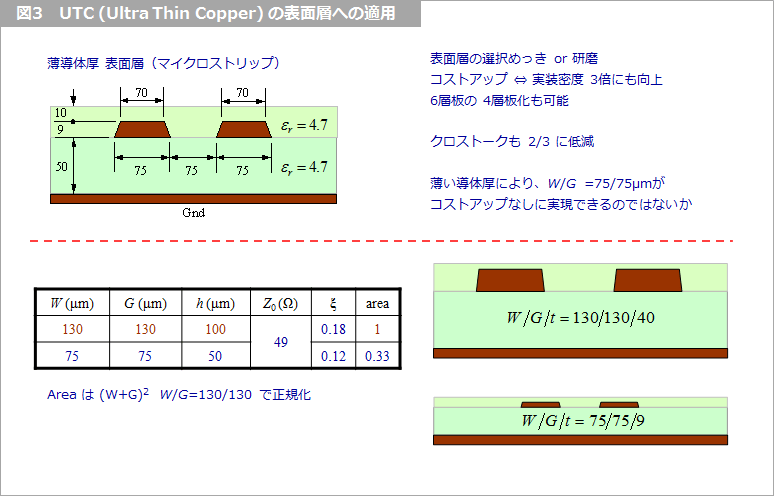
If we can make it as thin as W = 75 um, we can make the distance from GND 50 um and achieve Z0 = 50 Ω (Fig. 3, upper left diagram).
If G is also chosen to be 75 um, which is the same as W, the crosstalk coefficient can be reduced from 0.18 to 0.12 compared to W = G = 130 um (W = 75 um and W = 130um). It may be possible to reduce the number of layers by significantly improving the mounting density.
I would like to consider it and make it a reality, and I have been proposing it whenever I have the opportunity, but so far I have not received a report that it has been realized. My first reply when I made the proposal was to explain the reason why "selective plating", polishing, and etching are expensive, but I would appreciate it if someone could make it a reality.
Click here for recommended articles/materials
How to determine the cross-sectional dimensions of the board
Cross-sectional dimensions of the substrate surface layer - Part 1
Board differential transmission pattern design
Substrate Basic Knowledge Related Articles/Documents
======================================
What is Yuzo Usui's Specialist Column?
It is a series of columns that start from the basics of the basics, and include themes that you can't hear anymore, themes for beginners, and even a slightly advanced level, and describe them in as easy-to-understand terms as possible.
Maybe there are other themes that interest you!
Check out our other themed columns here.