
![]()
![]() Narrow down by specifying conditions
Narrow down by specifying conditions
現在1888件がヒットしています。check

Overview
High-frequency switches using wide bandgap semiconductors contribute to the efficiency of power conversion. Silicon carbide switches, for example, can be implemented as SiC MOSFETs or as SiC FETs in a cascode configuration.
This article traces the origins of SiC FETs, their evolution to the latest generation, and compares their performance with other technologies. In four installments, I will discuss the differences in physical characteristics, approaches and features for ideal switches, reliability, and unique uses in real-world applications.
Other SiC FET applications
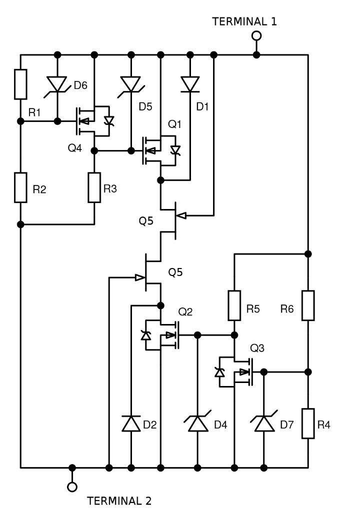
SiC FETs are suitable for high efficiency power converters and are available up to 1700V ratings for typical industrial three-phase applications. The cascode principle can be easily extended by "stacking" a SiC JFET onto a Si MOSFET for control (Figure 1). A module demonstrating this principle has been developed with a 40kV rating.
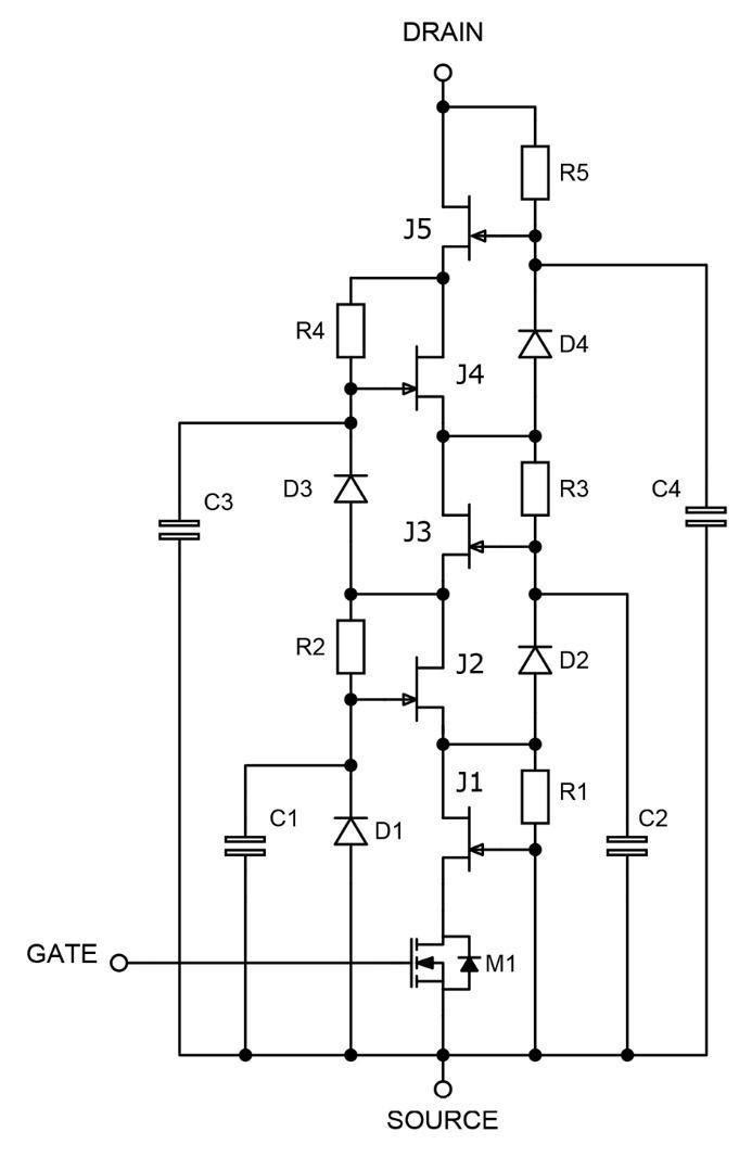
As mentioned earlier, SiC JFETs have a nearly constant saturation current characteristic with respect to gate-source-drain voltage, which can be used to advantage in circuit protection applications such as current limiters and breakers. Figure 2 shows the concept of a self-biased circuit protector using SiC FET cascodes. This circuit protector is a true "two terminal" that does not require external auxiliary power rails or internal DC-DC converters.
Progress towards improving performance and value
SiC FETs have gone through generations, with the latest GEN4 adding various improvements such as usable voltage range, cell density for improved on-resistance, and die sintering for improved thermal performance. Also, since the channel resistance is so low, conduction losses through the substrate become the limiting factor and substrate thinning techniques are used. Moreover, reduction of the output capacitance COSS in particular is achieved also on the dynamic side. This reduces losses in hard-switched continuous conduction modes like totem-pole PFCs, and enables high-frequency operation in soft-switched resonant circuits like LLCs and PSFBs.
Switching edge rates are now very fast, often called "ultra-fast" or deliberately low, to suit applications where the edge rate is not critical to performance and can cause EMI and failure issues such as motor drives. Devices are offered with a simple "fast" rating that slows them down to The packaging has also evolved from the original SiC FETs and is formed by placing Si MOSFET and SiC FET dies side by side and wirebonding them together. This has made it possible to flexibly support, for example, the TO-247 package, but in order to achieve high performance at a lower cost, a "stacked" package that uses a larger die and allows a large current to flow is needed. Die placement has become commonplace, especially when placing components side-by-side in compact modules.
Also, the solder die attach is replaced by sintered silver for improved thermal performance and the DFN8x8 package enables a low inductance high frequency layout for MHz switching. TO-220, TO-247 and D2PAK packages are still popular as they allow SiC FETs to be retrofitted to older designs using IGBTs. The 'Kelvin' source connection on the 4-lead versions of these packages alleviates problems caused by source lead inductance interfering with the gate drive loop. In addition to the increasing value of using SiC FETs for their electrical performance, we are also implementing cost reduction programs through ongoing production yield improvements and a move to 8-inch wafers.
Attractive Solutions SiC FETs
The latest generation of SiC FETs brings us a little closer to the ideal switch. It enables high-frequency power conversion stages with the lowest conduction and dynamic losses to date and efficiencies greater than 99%, with associated energy, size and weight savings. Designers are also pushing the definition of "ideal" to include stable performance over a wide range of operating and fault conditions, and easy to drive in a convenient package.
At the same time, equipment end-users are demanding highly reliable end products at a total lifetime cost that is a step up from older technology implementations. Qorvo's SiC FETs enable this with a range of parts with voltage ratings from 650V to 1700V and on-resistances up to 7mΩ. As a design aid, Qorvo's 'FET JET' calculator can quickly select and predict the performance of any of the company's devices in power conversion topology choices, including PFC stages and isolated/non-isolated DC-DC converters. I can.
Qorvo's "FET JET" calculator
Inquiry
If you have any questions regarding this article, please contact us below.
Qorvo manufacturer information top page
If you want to return to Qorvo manufacturer information top page, please click below.
