
![]()
![]() Narrow down by specifying conditions
Narrow down by specifying conditions
現在1888件がヒットしています。check

Overview
High-frequency switches using wide bandgap semiconductors contribute to the efficiency of power conversion. Silicon carbide switches, for example, can be implemented as SiC MOSFETs or as SiC FETs in a cascode configuration.
This article traces the origins of SiC FETs, their evolution to the latest generation, and compares their performance with other technologies. Over four times, the difference in physical properties, Approaches and Features for an Ideal Switch, reliability, Unique usage in real applications, will be explained.
Nearly perfect electrical switches have existed for a long time, of course, but we're not talking about mechanical switches here.
Modern power conversion ideally
・No resistance when on
・It has infinite resistance and withstand voltage when it is off.
・Simple drive
Arbitrarily fast, no instantaneous power dissipation
A picture with these conditions relies on a semiconductor switch that can switch between ON and OFF states.
In today's energy and cost sensitive world, these features enable high power conversion efficiency in power supplies, inverters, battery chargers, motor drives, etc. As a result, advantages such as smaller equipment size, lighter weight, lower failure rates, lower acquisition and lifetime costs, etc. can be obtained. Sometimes the entire application area is opened beyond the simple efficiency threshold. For example, an electric vehicle would be difficult to implement if the motor drive was lossy, resulting in a large and heavy vehicle that would require battery power with added weight and range penalties. Since the days of Shockley, Bardeen and Brattain 75 years ago, engineers have been refining solid-state switches to bring them closer to perfection.
Aiming for the ideal switch
The first power conversion applications certainly used mechanical switches. Mechanical "vibrators" were initially the only alternative to motor-generator sets for isolated DC-DC conversion and DC voltage boosting. However, about a decade after the transistor was invented, the first "switch-mode" power supplies (SMPS) appeared, and since then designers have had to take advantage of available semiconductor technology. The principle of the Field Effect Transistor (FET) was proposed and patented by Julius Edgar Lilienfeld in 1930, but could not be manufactured in practice and dominated early SMPS circuits primarily due to the use of germanium. It was a bipolar transistor.
The original bipolar transistors had limited voltage ratings, high off-state leakage, slow and lossy switching speeds, and required complex base drives. Even today, bipolar transistors for power have low gain and can require tens of amps of base current. Charge stored in the base has been a major problem limiting turn-off time and efficiency. Techniques were then used to limit the charge using techniques such as the "Baker clamp" to precisely tune the base drive and trade reduced conduction losses for dynamic losses.
Silicon "metal oxide gate FETs" or "MOSFETs" used vertical conduction paths and planar gate structures in the 70s and 80s, and "trench" arrangements in the 90s to Achieved high output. However, their use at high power was limited by the achievable voltage rating and on-resistance. IGBTs (Insulated Gate Bipolar Transistors), which appeared in the late 1970s, combine a MOSFET-like gate drive and a bipolar-like conduction path. The advantage is that the power loss increases nominally proportional to the current, rather than the square of the current as shown.
However, IGBTs also had problems. Latch-on phenomena can occur with catastrophic results. In addition, the "tail current" at switch-off caused relatively high dynamic losses, limiting the operating frequency. Modern IGBTs have solved the latch-up problem and minimized tail current. Also, the current and voltage ratings have improved dramatically, and they are often used for ultra-high power power conversion. However, due to dynamic losses, the switching frequency is limited to tens of kHz at most.
A high switching frequency is the key to miniaturization of magnetic circuits and miniaturization and weight reduction of power conversion products with high-performance control loops. Adoption of the "super junction" type reaching kHz is progressing. However, the breakdown voltage of silicon is a limiting factor, and bulk material thickness must be minimized for a given operating voltage, resulting in high on-resistance (RDS). To reduce this, many cells must be parallelized, which increases the total die area (A).
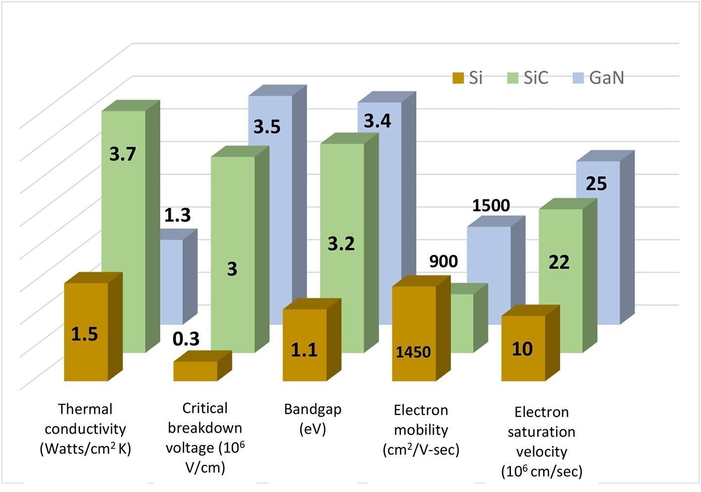
This effect is quantified by a “figure of merit” of on-resistance per unit area (RDSA). As a result, interest in the wide bandgap materials silicon carbide (SiC) and gallium nitride (GaN) is increasing. These materials not only have high intrinsic breakdown voltages, but also have other favorable properties such as electron mobility, saturation velocity, high temperature resistance and, in the case of SiC, improved thermal conductivity. Figure 1 compares the headline characteristics of silicon, SiC, and GaN materials.
Early stage of SiC device development
Development of SiC devices began a decade earlier than GaN, and was expected to see broader application to higher voltage and power ratings. A natural starting point for SiC switches was to consider the development of enhancement-mode normally-off MOSFETs for compatibility with existing Si MOSFET designs and manufacturing techniques. As with any new technology, some problems were expected and some were not, delaying the product launch.
Compared to silicon, SiC has more lattice defects and lower electron mobility at the interface between the gate oxide film and the SiC channel, resulting in a relatively high on-resistance. To be cost effective, SiC wafer size must be maximized, but industry standard 6-inch wafers have difficulty maintaining low defect rates and wafer flatness.
SiC MOSFETs also have unstable gate thresholds and high hysteresis, making it difficult to design a gate drive for optimum efficiency and reliability. Modern SiC MOSFETs have improved performance and can theoretically be driven unipolar from 0 to 15V, but in practice use a negative gate voltage of -5V for reliable operation. I often do Also, since 15V does not provide the lowest on-resistance, 18V is often used to improve efficiency, but at the cost of reduced short-circuit resistance and a margin for the typical absolute maximum voltages of 19V and 20V. decrease. Other issues include deterioration of the gate oxide film during short circuits and overvoltage, and excessive electric field stress on the gate oxide film due to the high electric field strength between the drain and gate when the device is in a blocked state.
Around 2010, an unexpected problem occurred with SiC MOSFETs. These are lattice bulk defects called basal plane dislocations, which actually grow and migrate under stress during operation. When the body diode from source to drain is conducting, electron and hole carriers are generated and move with enough energy to recombine and propagate the defect. This is due to the high energy value of SiC's bandgap, which results in an increase in leakage current and on-resistance, leading to deterioration that leads to increased losses and failures. Today's SiC MOSFETs have greatly improved due to advances in manufacturing methods and defect screening, but efforts continue to improve die yield, cost effectiveness, and package performance such as low inductance and thermal resistance. .
Inquiry
If you have any questions regarding this article, please contact us below.
Qorvo manufacturer information top page
If you want to return to Qorvo manufacturer information top page, please click below.
