- Semiconductor BusinessHOME
- Products and Services of Macnica,Inc.
-
technical information

-
Events and Seminars
- Handling Manufacturer
- Support
- Inquiry
- Click here to purchase products
- Semiconductor business e-mail magazine registration
![]()
![]() Narrow down by specifying conditions
Narrow down by specifying conditions
現在2182件がヒットしています。check

This is an updated version of the old title "DS-5 Utilization Technique - Register View [2/3] Self-made register definition".
Arm® Development Studio for Intel® SoC FPGA Edition (Arm® DS ) has been changed to Arm® DS is the successor to DS-5, and usability does not change significantly. Most of the content in this series of articles can be applied to both Arm® DS / DS-5, but where there are differences, we have updated them to that effect.
***
This article provides supplementary information on how to use Arm® DS / DS-5, which can be used as a software integrated development environment for Intel® SoC FPGAs.
Arm® DS / DS-5 for Intel® SoC FPGA will be a product called "Intel® SoC FPGA Edition". The difference between the Intel® SoC FPGA edition and the Arm® genuine edition is only the supported devices to be connected, and there is no difference in how to use the debugger and attached tools (compiler/linker, etc.). Therefore, basically, by referring to the Arm® DS / DS-5 manuals published by Arm®, you can understand how to use it in general.
Arm® Development Studio documentation page (Arm® Developer site)
DS-5 Documentation Page (Arm® Developer Site)
This time, I will post how to add a new display item (register definition) to the register view of Arm® DS / DS-5.
Peripherals that do not support register display
The Arm® DS/DS-5 register view pre-defines registers for various peripherals documented in the HPS Technical Reference Manual. Register display is possible only by selecting the display items described in the previous article.
However, for peripherals implemented using Arm® IP, some detailed register definitions are not done, so it is not possible to set/check values using the register view.
It does not support register display of the following peripherals.
* DMA Controller (DMA-330)
* L2Cache Controller (L2C-310)
* Cortex-A9 MPCore built-in SCU (Snoop Control Unit)
* Cortex-A9 MPCore Built-in Interrupt Controller (GIC: PL-390)
* Cortex-A9 MPCore built-in Timer (GlobalTimer, PrivateTimer, WatchdogTimer)
For peripherals that do not support the display of the register view, the detailed specification of the register is not described on the register map, and the base address and the link to the reference document are described.
Reference: Cyclone® V SoC HPS Address Map and Register Definitions
How to add register definitions
By describing register definitions in .svd format or .tcf format (both are XML-based file formats), you can freely define registers that correspond to the register view display.
The register definitions that are displayed initially are also stored under the Arm® DS / DS-5 installation directory, so you can refer to them when writing .tcf. (Definitions for other devices are also stored in nearby directories)
[Arm® DS / DS-5 Install Directory]/sw/debugger/configdb/SoCs/altera/hps_svd.tcf
As a reference for .svd, files in .svd format are stored under the installation directory of the Intel® Quartus® Prime software.
[Intel® Quartus® Prime Install Directory]/ip/altera/hps/altera_hps/altera_hps.svd
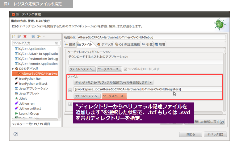
Specify the location of the described register definition file by selecting "Add peripheral description file from directory" on the file tab of the debugger connection settings (debug configuration) of Arm® DS / DS-5. By doing so, the register definitions will be loaded when the debugger is connected. No special settings are required other than this specification.
Below is an image of the setting screen for specifying the register definition file.
Difference between .svd and .tcf
Select either .tcf or .svd for the format of the register definition file.
The .svd is standardized as the System View Description (SVD) within the Cortex Microcontroller Software Interface Standard (CMSIS). The XML format is also published as a CMSIS document.
The Intel® SoC FPGA Embedded Development Suite (SoC EDS) User Guide also only describes how to use .svd, so .svd seems to be the recommended format. (.tcf format is not mentioned in the user guide)
Reference: Cortex Microcontroller Software Interface Standard (CMSIS)
On the other hand, the recommended format for Arm® DS / DS-5 seems to be .tcf.
The Arm® DS / DS-5 documentation also describes it as a Target Configuration File (TCF), which has the advantage of having a dedicated editor for editing.
Reference: Arm® Development Studio User Guide "Working with the Target Configuration Editor"
Reference: Arm® DS-5 Debugger User Guide "Working with the Target Configuration Editor"
Even register definitions created in .svd format seem to be automatically converted to .tcf format when Arm® DS / DS-5 reads the register definition file. After all, the automatically converted .tcf will be used, so you can choose which format you want to create register definitions in.
Personally, I prefer .tcf.
Not only is there an editor for editing, but even if you edit the XML directly with a text editor, I feel that the .tcf XML has a tag structure that is easier to edit.
The details of the description method (XML tag structure) are beyond the scope of this article. Please refer to existing definition files and documents when writing.
Sample register definition file
Here is a .tcf file that describes a set of register definitions for Arm®-related peripherals that are not supported by the Arm® DS / DS-5 register view. Please use it as a reference for the description contents of the register definition file.
It is written so that it can be used as is for debugging Cyclone® V SoC / Arria® V SoC, but we do not guarantee that the content is correct. (Use at your own risk)
soc_cv_av_hps_addon_dma330__2.tcf
Register definitions for DMA Controller (DMA-330)
soc_cv_av_hps_addon_mpul2_l2c310__1.tcf
Register definitions for L2Cache Controller (L2C-310)
soc_cv_av_hps_addon_mpuscu__2.tcf
Register definitions for Cortex-A9 MPCore integrated peripherals
I also created a version with a modified base address definition for the Intel Arria 10 SoC.
(Please use this at your own risk.)
soc_a10_hps_addon_dma330__1.tcf
Register definitions for DMA Controller (DMA-330) [for Intel® Arria® 10 SoC]
soc_a10_hps_addon_mpul2_l2c310__1.tcf
Register definitions for L2Cache Controller (L2C-310) [for Intel® Arria® 10 SoC]
soc_a10_hps_addon_mpuscu__1.tcf
Register definitions for Cortex-A9 MPCore integrated peripherals [for Intel® Arria® 10 SoC]
This time, I described how to make your own Arm® DS / DS-5 register definition.
In the next (final) time, I will describe how to display the registers on the FPGA side.
Click here for recommended articles/materials
Arm DS Utilization Technique - Register View [1/3] Basic Settings
Arm DS Utilization Technique - Register View [2/3] Self-made register definition
Arm DS Utilization Technique - Register View [3/3] Register display on FPGA side
List of articles on Arm DS utilization
SoC FPGA related articles and resources
Intel® FPGA SoC FPGA
Intel® FPGA Development Flow/FPGA Top Page