- Semiconductor BusinessHOME
- Products and Services of Macnica,Inc.
-
technical information

-
Events and Seminars
- Handling Manufacturer
- Support
- Inquiry
- Click here to purchase products
- Semiconductor business e-mail magazine registration
![]()
![]() Narrow down by specifying conditions
Narrow down by specifying conditions
現在2183件がヒットしています。check

This is an updated version of the old title "DS-5 Utilization Technique - Register View [3/3] Register display on the FPGA side".
Arm® Development Studio for Intel® SoC FPGA Edition (Arm® DS ) has been changed to Arm® DS is the successor to DS-5, and usability does not change significantly. Most of the content in this series of articles can be applied to both Arm® DS / DS-5, but where there are differences, we have updated them to that effect.
***
This article provides supplementary information on how to use Arm® DS / DS-5, which can be used as a software integrated development environment for Intel® SoC FPGAs.
Arm® DS / DS-5 for Intel® SoC FPGA will be a product called "Intel® SoC FPGA Edition". The difference between the Intel® SoC FPGA edition and the Arm® genuine edition is only the supported devices to be connected, and there is no difference in how to use the debugger and attached tools (compiler/linker, etc.). Therefore, basically, by referring to the Arm® DS / DS-5 manuals published by Arm®, you can understand how to use it in general.
Arm® Development Studio documentation page (Arm® Developer site)
DS-5 Documentation Page (Arm® Developer Site)
This time, I will post how to display the registers on the FPGA side in the register view of Arm® DS / DS-5.
Automatic generation of register definition file
When you create a hardware design for SoC FPGA using Platform Designer (formerly Qsys), a register definition file (.svd) is automatically generated.
Auto-generated location
[Quartus Project Directory]/soc_system/synthesis/soc_system_hps_0_hps.svd
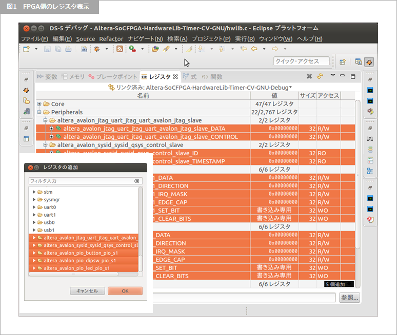
By loading the above register definition file into Arm® DS / DS-5 in the same way as the content posted in the previous article, it is possible to display the registers on the FPGA side in the register view. (Select "Add peripheral description file from directory" in debug configuration)
Below is an image of the register view showing the registers on the FPGA side.
By the way, if you read both the automatically generated register definition and the sample register definition (.tcf) posted in the previous article, many warning messages starting with "Warning (TAD231): xxxx " will be displayed, but these It's okay to ignore everything.
These messages are displayed when the name of the peripheral used in the register definition file is duplicated. In the sample register definition (.tcf), additional register definitions are written for the peripherals (dmanonsecure, dmasecure, mpul2, mpuscu) defined from the beginning, but the automatically generated register definitions (. svd) also has a peripheral with the same name, so if you read both register definitions, it seems to warn of duplication.
IP components with register display support
Register definitions are automatically generated for Platform Designer (formerly Qsys) IP components that support register definition files (CMSIS-SVD).
Regarding CMSIS-SVD support of IP components, there is some explanation in the Intel® Quartus® Prime Software User Guide - Platform Designer document, but it is not enough, so it seems good to refer to existing IP components. .
Reference: Intel® Quartus® Prime Standard Edition User Guide - Platform Designer
Reference: Intel® Quartus® Prime Pro Edition User Guide - Platform Designer
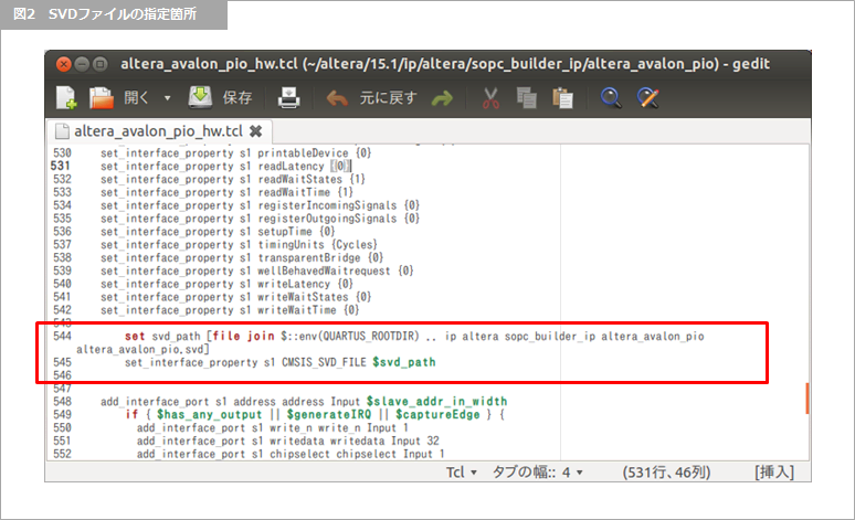
For reference, when I checked the IP component (PIO) file that supported CMSIS-SVD, I was able to confirm that CMSIS_SVD_FILE was set as an Interface Property in the _hw.tcl file.
The description in the blue frame in the image below is the corresponding description.
If you want to create an IP component that supports CMSIS-SVD, the following seems to be necessary.
* Prepare a register definition file in .svd format.
* Write to _hw.tcl to specify CMSIS_SVD_FILE with set_interface_property.
On the community site (Rocketboards.org) that distributes information related to Intel® SoCFPGA
For more detailed information, please refer to the document page linked below.
Reference: Using CMSIS with Custom FPGA Logic
References to registers not supported by the register view
It also mentions how to reference the desired register without adding a register definition. In addition to the register view, it is also possible to refer to registers using the windows below.
* expression view
* memory view
Below is an image showing how to refer to registers in each view.
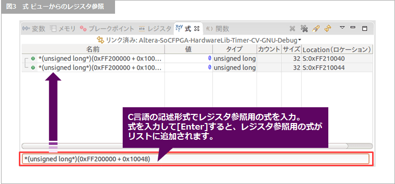
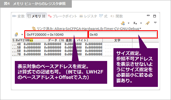
Up to this point, we have described how to customize the register view, but if the register definition is troublesome, you can refer to the register using the method shown in the image above.
We have posted about how to use the register view of Arm® DS / DS-5 in three parts, but this article will be the final article about the register view.
Click here for recommended articles/materials
Arm DS Utilization Technique - Register View [1/3] Basic Settings
Arm DS Utilization Technique - Register View [2/3] Self-made register definition
Arm DS Utilization Technique - Register View [3/3] Register display on FPGA side
List of articles on Arm DS utilization
SoC FPGA related articles and resources
Intel® FPGA SoC FPGA
Intel® FPGA Development Flow/FPGA Top Page