- Semiconductor BusinessHOME
- Products and Services of Macnica,Inc.
-
technical information

-
Events and Seminars
- Handling Manufacturer
- Support
- Inquiry
- Click here to purchase products
- Semiconductor business e-mail magazine registration
![]()
![]() Narrow down by specifying conditions
Narrow down by specifying conditions
現在2176件がヒットしています。check

open-loop transfer function
To understand why this happens (the peak in Figure 17), consider the open-loop transfer function A0β in Figure 18. R0 is the op amp output resistance, which is 75Ω for the μA741. For a gain of 2, set R1=R2=100kΩ.
As shown in the formula in Figure 18, β is the primary lag circuit. The constant term in the denominator of this delay circuit is the cutoff frequency (angular frequency) ω3 of the delay circuit, which in this example is 212kHz.
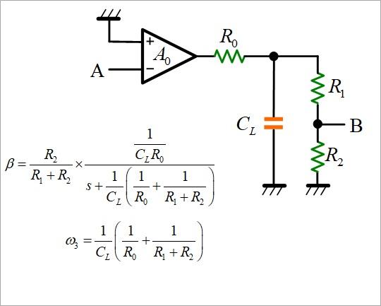
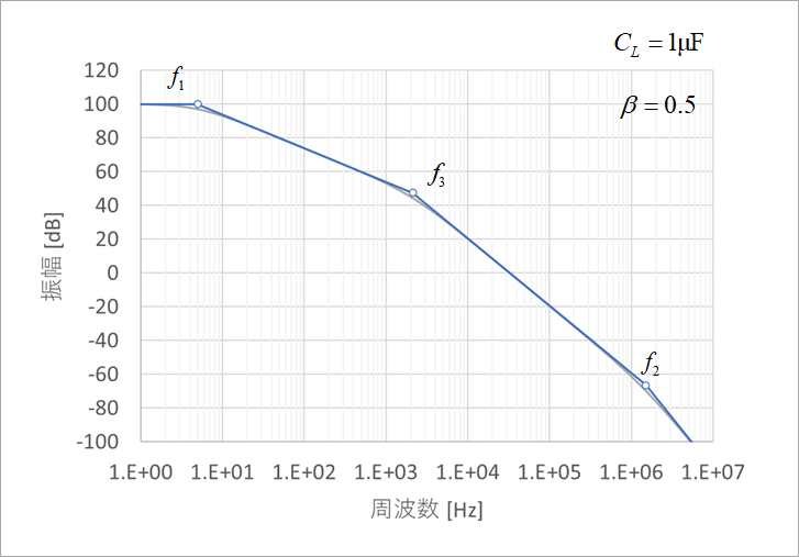
Fig. 19 shows the frequency characteristics of Aβ with a broken line. f3 in the same figure is the cutoff frequency of the β delay circuit.
In order to determine the stability of this circuit, the amplitude characteristics in Fig. 20(a) and the phase characteristics in Fig. 20(b) are used. Now consider CL=1µF, R1=R2, or β=0.5, gain of 2. The point where the gain becomes 0 dB in Fig. 20(a) is 32.5 kHz, and the phase at this time is -177.5° from Fig. 20(b), and the phase margin PM from -180° is only 2.5°. As a result, the time response oscillates as shown in Fig. 16(b). The difference can be seen when compared with Figure 9(b), which has a phase margin of 72°.
These two graphs of gain and phase are called Bode line, and it is one method of determining the stability of the system. Since this circuit has three stages of delay circuits, the final phase will be smaller than -180° (larger negative). The point where -180° crosses is 56.5 kHz from Figure 20(b). Go back to Figure 20(a) and read the -9.6dB gain at 56.5kHz. This value of 9.6 dB below 0 dB of gain is called the gain margin GM. The guidelines for gain margin GM and phase margin PM differ depending on the purpose of the circuit, but usually 20 dB for GM and 60° for PM are sufficient.
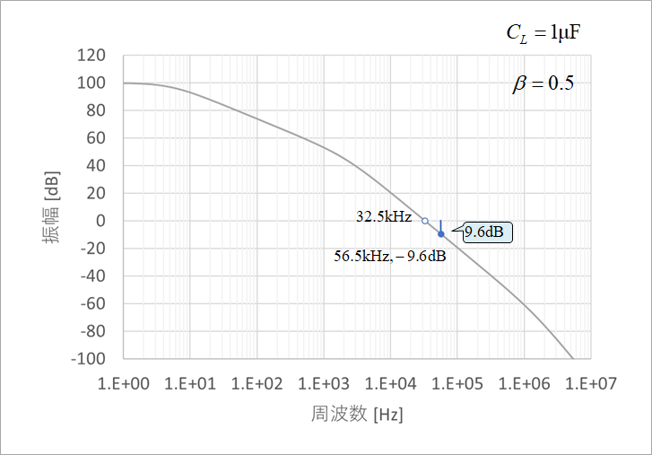
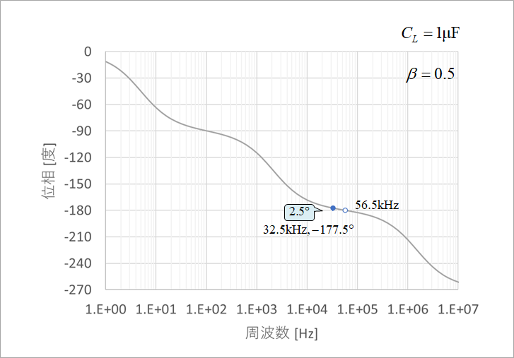
Figure 21 shows the calculated phase margin versus load capacitance for this circuit. As CL is reduced, it eventually approaches 72° at no load. From the same figure, the load capacitance CL when the phase margin PM is 60° is 0.001μF.
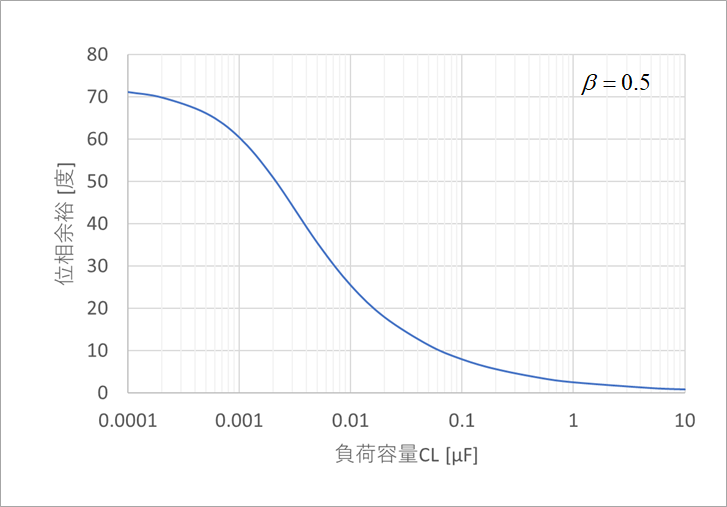
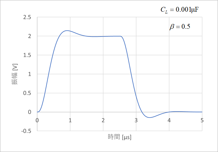
Figure 22 shows the response waveform at this time.
The problem of oscillation due to capacitive loads has been a common occurrence in the past, and I have received many inquiries about it. This comes from the "belief" that adding capacitance suppresses vibration and oscillation. Always keep in mind that capacitive loads in negative feedback circuits can cause oscillations. Similar oscillation problems arise in emitter follower and source follower circuits.
This example was given as a capacitive load on a normal op amp. In general, I don't think it's common to connect a 1uF capacitive load to the output of an op amp. If a circuit similar to an op amp is used at the output of the power supply, the output resistance will be around 0.1Ω, for example. It's three orders of magnitude smaller than the op amp example, so a 1 µF load in this example is equivalent to 1,000 µF at the power supply. A similar analysis can be performed by changing the operational amplifier model (output resistance).
Example solution for stabilization
Waveform oscillation is caused by phase lag.
It's an easy-to-understand parable, half joking, but see "Digression 2".
As a countermeasure, the phase delay should be advanced in the opposite direction.
The basic form of the phase lead circuit is shown in Fig. 1(b).
A form close to this is incorporated into the open-loop transfer function.
Add a series circuit of resistor RS and capacitor CS in parallel with feedback resistors R1 and R2 in Figure 23. Figure 1(b) shows only the feedback circuit. The transfer function F(s) of this circuit is shown in the figure. An example with RS and CS values of RS=10kΩ and CS=60pF is described.
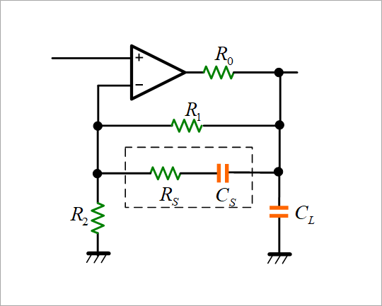
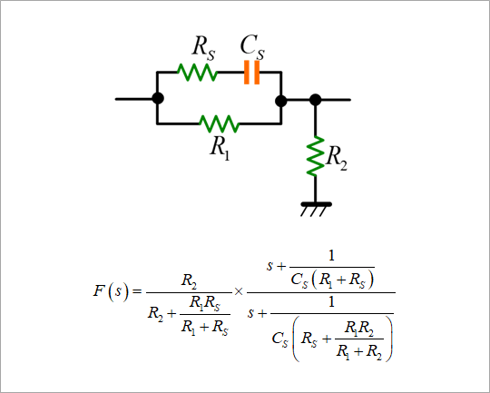
Figure 24 shows the phase characteristics of the phase lead circuit for the above constants in Figure 23.
A phase lead of about 17° can be obtained in the frequency band of several 100 kHz.
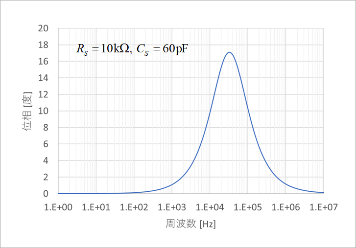
Fig. 25 compares the phase characteristics of the open-loop transfer function Aβ with and without the lead circuit. It's not enough, but it gives us a phase margin of 18.5°.
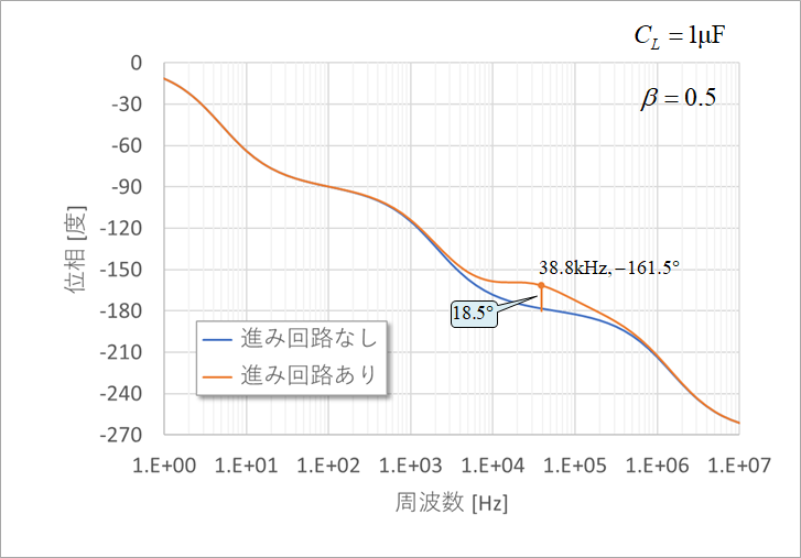
Figure 26 shows the output waveform when the lead circuit is added. Comparing with Fig. 16, we can see that the vibration is suppressed.
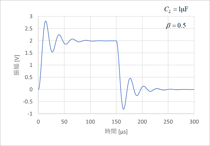
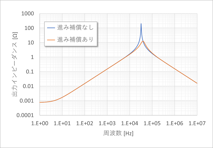
Figure 27 shows the closed-loop gain with capacitive load, with and without lead compensation. The gain has a large peak near the zero-cross frequency of A0β. Adding lead compensation can dampen that peak.
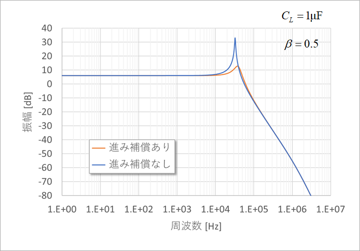
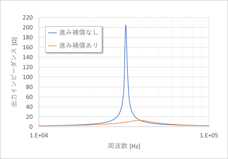
Figure 28 shows the output impedance with and without lead compensation when the load capacitance CL = 1 µF. In (a), the vertical axis is on a logarithmic scale, and the peak value does not seem to differ much, but in (b), where the vertical axis is on a linear scale, you can see the difference in output impedance with and without lead compensation.
Nyquist stability decision
In addition to the Bode plot stability criterion, there is also the Nyquist stability criterion (footnote 4). Display the magnitude and phase of the Bode plot in polar coordinates.
Figure 29(a) is drawn in the direction of the arrow from 1Hz to 10MHz. What is needed for Nyquist discrimination is data whose phase is around -180°. (b) of the same figure extracts only this necessary range (33kHz to 10MHz). The point where this curve intersects the horizontal axis is the point where the imaginary part of the amplitude is zero, or the phase is -180°. This corresponds to 56.5kHz in Figure 20(b). An instability condition is a gain of 0 dB or greater than 1 at this point.
In other words, the trajectory passes to the left of (-1,0) in Fig. 29(b). In (b) of the same figure, the zero cross point is around -0.33, so the state is quite unstable.
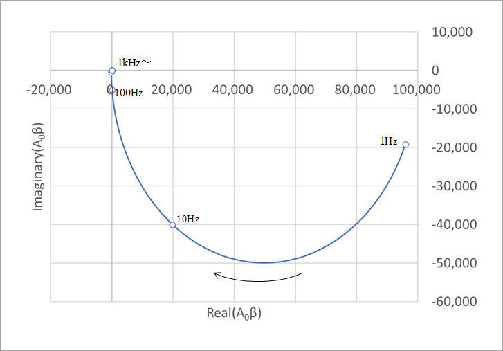
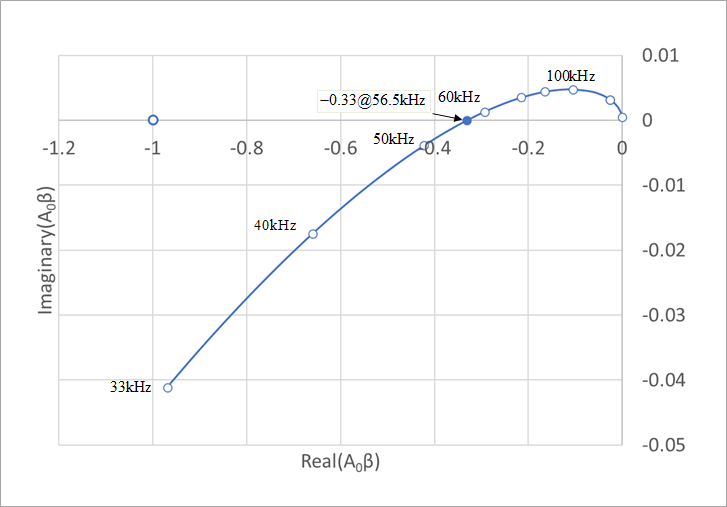
Figure 30 is the Nyquist plot with lead compensation. The zero cross point is far from (-1,0) and almost close to the origin (0,0), so it can be judged stable.
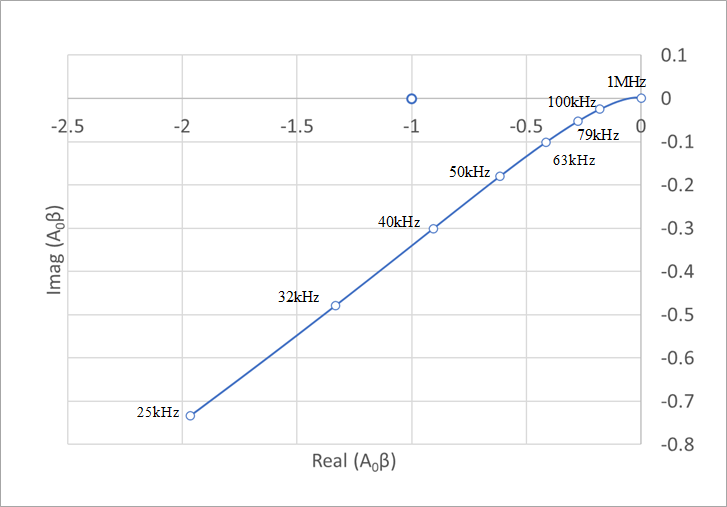
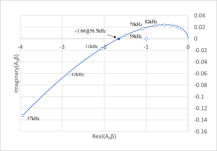
Figure 31 is an example of deliberately creating an unstable condition. When the capacitive load is 1 μF, the GB product of the operational amplifier is assumed to be 5 MHz. The trajectory passes through the point (-1,0) looking inside or to the right. In this condition the circuit goes into oscillation.
To determine the stability of the feedback circuit, it is best to choose either the Bode plot or the Nyquist plot, whichever is easier.
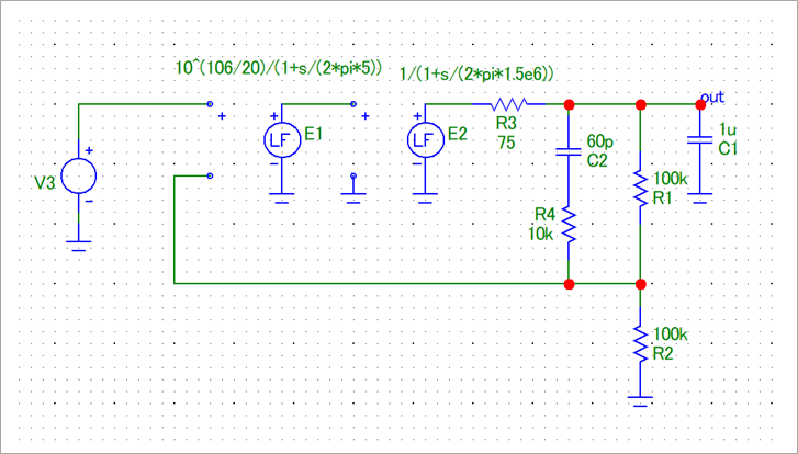
For the analysis in this paper, the frequency formula was set up and calculated with Excel, and the time response was obtained with FFT. For verification, it was also parsed with SPICE. Figure 32 is a SPICE analysis circuit.
The operational amplifier used Laplace's signal source (Laplace formula VofV). The delay circuit combined 1/(1+s/ω1) and 1/(1+s/ω2) with a DC gain of 106dB, 10^(106/20). Other than that, I don't think any further explanation is necessary.
Footnote 4
This is a stability determination method for feedback systems devised by Swedish physicist Harry Nyquist.
Nyquist is also credited with the sampling theorem (Nyquist frequency) and thermal noise.
"Digression 2"
This is not my area of expertise, so it's just speculation, so go for it.
It is the negative feedback circuit that allows humans to ride a bicycle and run straight.
When you're about to go right, your brain tells you to correct it to the left. Since the command is issued without delay, you can run smoothly.
The following is illegal and dangerous, so please treat it as an example only.
Riding a bike while drunk makes me dizzy. In severe cases, it will almost fall on the side of the road, return to the center, and then fall on the other side.
The reason for this is considered to be the delay in the control circuit.
Even if it is about to go to the right, the command is delayed and the control cannot keep up, so it goes to the right. When you go too far, the command arrives late and you take the steering wheel to the left.
The greater the lag, i.e. the greater the degree of drinking, the greater the vibration.
I was half joking, but I think I can understand the cause of the vibration in theory.
Drunk driving is dangerous because it delays judgment. Please do not ride after drinking.
What is Yuzo Usui's Specialist Column?
It is a series of columns that start from the basics, include themes that you can't hear anymore, themes for beginners, and also a slightly advanced level, all will be described in as easy-to-understand terms as possible.
Maybe there are other themes that interest you!