- Semiconductor BusinessHOME
- Products and Services of Macnica,Inc.
-
technical information

-
Events and Seminars
- Handling Manufacturer
- Support
- Inquiry
- Click here to purchase products
- Semiconductor business e-mail magazine registration
![]()
![]() Narrow down by specifying conditions
Narrow down by specifying conditions
現在2184件がヒットしています。check

Basic characteristics of operational amplifiers
In order to investigate the cause of the overshoot in Fig. 9(a), we will first review the characteristics of operational amplifiers.
Here we consider the most basic, the μA741. The μA741 is historically the first general-purpose op amp that does not require special compensation circuitry. The analysis below is based on a model created by the author by estimating from the manufacturer's data sheet, and may differ slightly from the actual device characteristics.
The operational amplifier came to be Op Amp, combining the English words Op and Amp for Operational Amplifier. It's a somewhat Japanese abbreviation, but it's almost the same as the English pronunciation. The reason for "calculation" is that operational amplifiers can be used to implement circuits for addition, subtraction, multiplication and division (footnote 2) and calculus. It has the name "calculation" in the sense that it constitutes an arithmetic circuit. You can easily find the solution by combining the differential equations as they are. This was called an analog computer and was used for practical and educational purposes until the early 1970s. There was a time when complex differential equation transients were easier to solve on an analog computer. (Footnote 3)
ideal op amp
What is an ideal operational amplifier?
(1) Infinite gain
(2) Infinite input impedance
(3) Zero output impedance
(4) Zero input offset voltage
However, real op amps are far from ideal.
Of the above features, (2) has an input current (called a bias current) on the order of picoamperes (pA) to microamperes (μA), depending on the IC process. Op amp circuits use a combination of resistors, but if the resistor values are asymmetrical with respect to each input terminal, and if large resistor values are used, a difference in voltage drop will occur due to the input bias current. An error will occur in the output voltage.
Also, even if this resistance value is set symmetrically, if there is a difference in the bias current depending on the input terminal, an error will occur as well. The offset voltage in feature (4) above is caused by the difference in the characteristics of the input differential pair transistors. products are also available.
op amp gain
Here, the gain of (1) has a particularly large effect, so we will discuss it in detail.
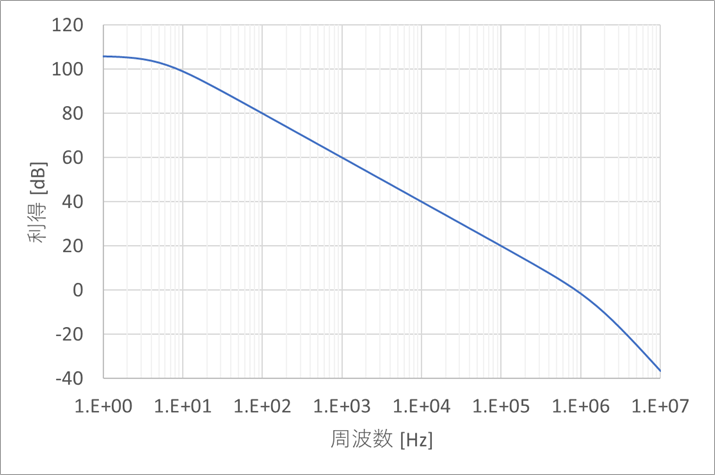
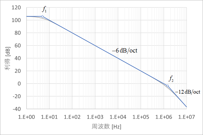
Fig. 10(a) is the bare amplitude characteristic without feedback. It is also called open loop or open loop because it does not apply feedback. Fig. 10(b) shows this in broken line notation. There are two points where the slope of the characteristic changes (roll-off points). One is a very low frequency f1, in this case 5Hz. The other is f2 just above the zero crossing (0dB gain) point, in this case 1.5MHz.
It rolls off in a straight line from f1 to near the zero cross point. This slope is -6dB/oct or -20dB/dec for first order lag circuits.
At frequencies above f2, the slope doubles (2nd order lag) to -12dB/oct or -40dB/dec.
The linear portion between f1 and f2 has a constant product of gain (dB) and frequency. For example, 80dB (10^4) at 100Hz (1.E+02) and 40dB (10^2) at 10kHz (1.E+04) both give a product of 10^6, or 1MHz. This is called the gain bandwidth product (GBWP: Gain Band Width Product). The unit is Hz.
In this case, the DC gain is 106dB (2×10^5), so it can be regarded as almost infinite, but as can be seen from Figure 10, the gain becomes smaller at higher frequencies.
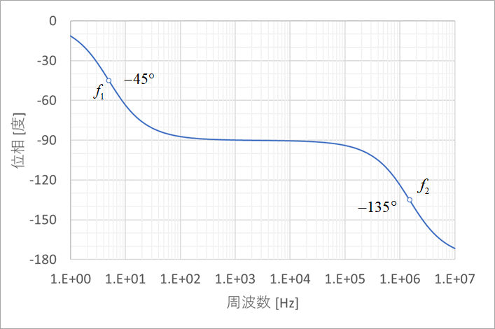
Figure 11 is also the bare phase response. -45° at lower frequency f1, then stays at -90° for a while, then another -45° at next f2, i.e. -135°, heading towards -180°. In other words, it can be seen that an operational amplifier is a combination (cascaded connection) of first-order lag circuits with two cutoff frequencies, a low frequency of several Hz and a high frequency above the zero-cross frequency. This phase characteristic is represented by the arctangent, -arctan(f/f1)-arctan(f/f2).
Feedback loop characteristics
To determine the stability of this system, we use the loop gain (A0β), shown in Figure 7. This A0β goes around the feedback loop, so it is called the open-loop transfer function. The gain from input to output is the opamp's bare gain, A0, and β times this is returned to the input. The gain of this round is A0β, the product of A0 and β.
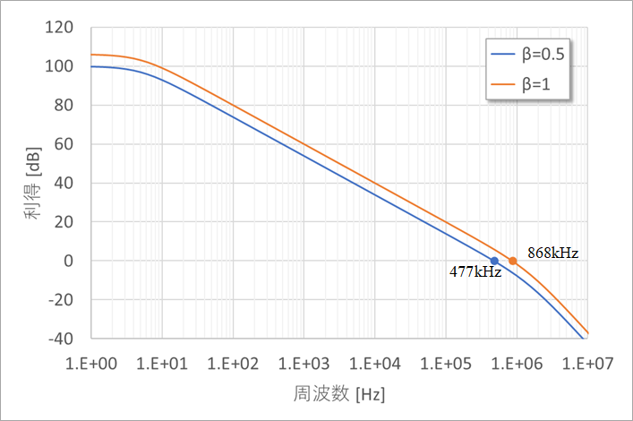
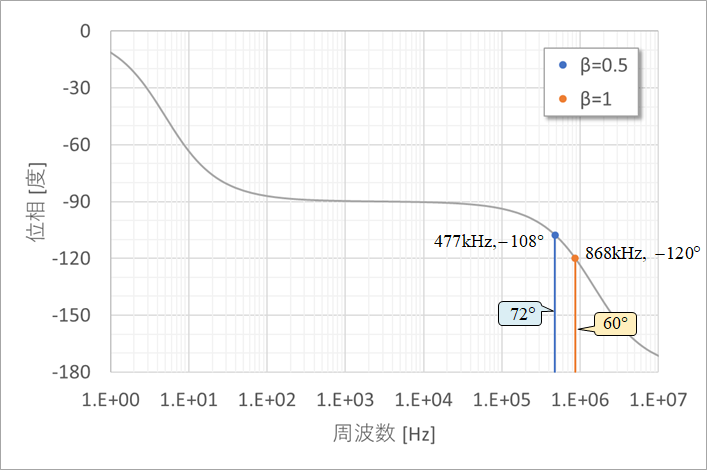
Figure 12 shows the amplitude characteristics of A0β, and Figure 13 shows the phase characteristics.
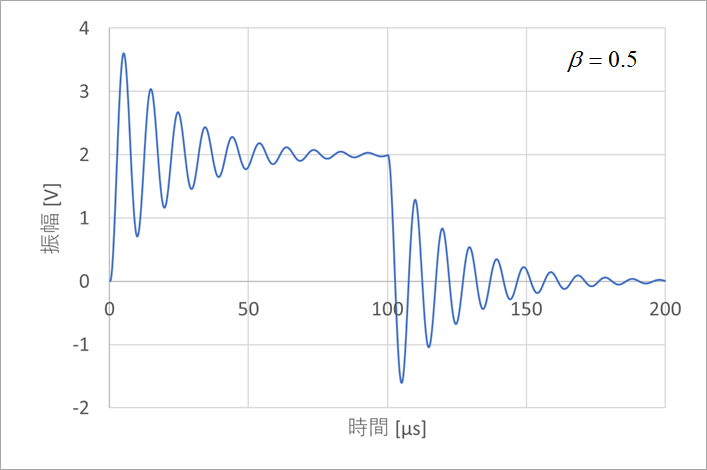
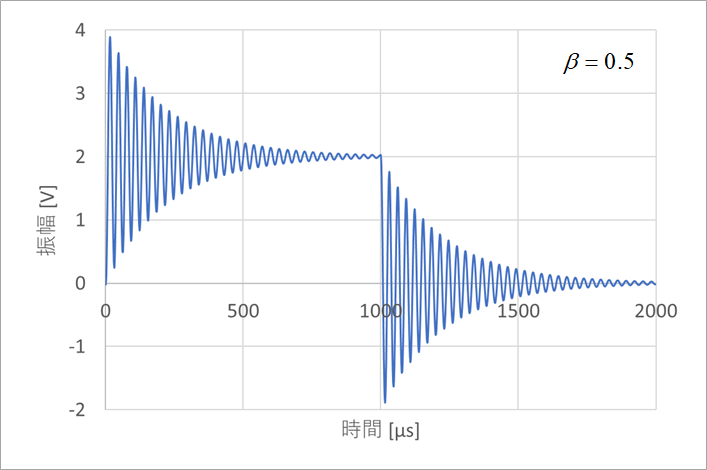
β=1 (G=1 in Fig. 9(a)) and β=0.5 (G=2 in Fig. 9(b)) are shown.
The phase characteristics in Figure 13 are the same as the characteristics of the operational amplifier alone (Figure 11) because β does not have frequency characteristics, and there is no difference due to the value of β.
For β=1, A0β=0dB at 868kHz from Fig. 12, that is, the round-trip gain is 1.
At the zero-crossing frequency of this amplitude, the phase is -120° from Figure 13. The difference between this phase and -180 is called Phase Margin (PM) in the sense of margin for oscillation. In this example PM=60°. -180° means that the phase is reversed, so negative feedback actually becomes positive feedback.
The phase margin for β=0.5 is 72° and more margin for β=1. This difference in phase margin is the difference in the time responses in Figs. 9(a) and (b). In this case, the phase does not reach -180°, but when it reaches -180°, oscillation will occur if the gain at -180° exceeds 0dB. How small this gain is relative to 0dB is called gain margin (GM).
The combination of Figures 12 and 13 is called a Bode diagram (or Pode diagram), and is a representative method for determining the stability of the feedback system.
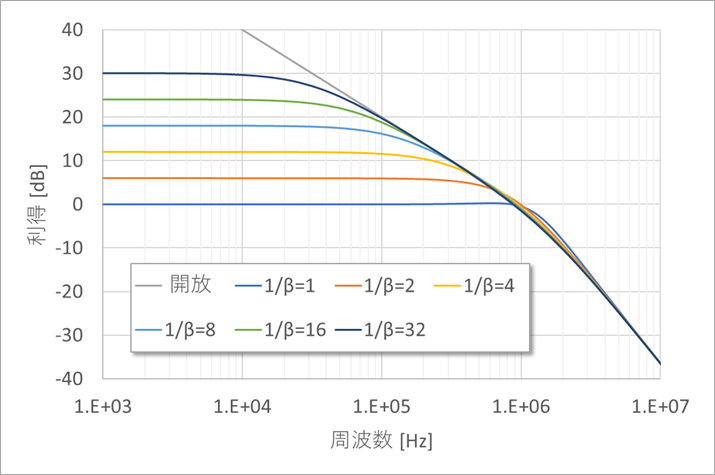
Closed-loop frequency response
Figure 14 is the closed-loop amplitude characteristic. The characteristic is flat up to several 100kHz, and after that, it finally approaches a 2nd order roll-off characteristic of -12dB. The gain in the plateau is 1/β. For example, if 1/β=8 then 20log(8)=18dB. At frequencies slightly above the roll-off point in the figure, the gain is greater than the open-loop characteristic. This is because in this region, due to the phase lag, the feedback is more positive than negative. The higher 1/β, i.e. the higher the gain, the lower the roll-off point.
op amp output impedance
Finally, let's talk about feature (3) output impedance. The bare output impedance of a normal op amp is on the order of several ohms to tens of ohms. This mainly depends on the size of the output transistors. As mentioned before, a negative feedback circuit has a lower output impedance. If the DC output impedance is R0, the output impedance when feedback is applied is R0/(1+A0β), which is inversely proportional to the closed loop gain.
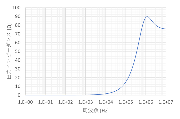
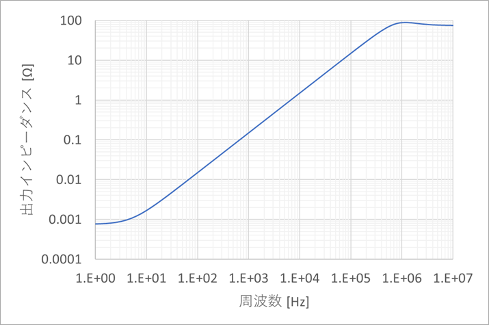
Figure 15(a) shows the output impedance versus frequency on a linear scale. It is several ohms or less up to around 10kHz, but from around 1MHz, it becomes a value of the bare output impedance.
Figure 15(b) shows the vertical axis on a logarithmic scale. Although it is on the order of mΩ for direct current, it increases linearly with increasing frequency.
Operation when load capacity is applied
Especially in the case of power supply circuits, it is desirable to lower the output impedance at high frequencies, so in many cases a capacitor is connected to the output. First, what happens to the time response when a capacitor is connected to the output? I feel that the waveform is dull depending on the capacitance.
However, the result of the analysis is the vibration waveform shown in Fig. 16. Figure 16(a) is for a load capacitance of 0.1 µF, and (b) is for 1 µF. Please note that the time axis differs between (a) and (b).
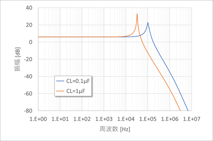
Figure 17 shows the closed-loop amplitude characteristic with load capacitance. Although it shows a large peak, the frequency showing this peak matches the vibration frequency in Fig. 16.
The purpose of this paper is to understand why the waveform oscillates in the time response and the amplitude peaks in the frequency response. Next time, I will discuss these in detail.
脚注2:
Multiplication circuits, for example, required multi-step operations using shifters and accumulators in early digital operations. In analog, using the exponential characteristics of bipolar transistors, it was possible to instantaneously obtain the product as log(x)+log(y)=log(xy). Analog arithmetic was much faster at this stage.
Footnote 3:
When solving a differential equation with a digital computer, it is basically a difference equation and solved by setting the increment Δt. If the steps were set smaller than necessary, errors would accumulate and an accurate solution could not be reached, or because the computing power of early computers was not high, it would take a huge amount of computation time. I had a hard time setting the increments because coarser increments have accuracy issues.
Even now, when using the circuit analysis software SPICE, I think that the notch problem is a hardship.
Analog computers, on the other hand, don't have the ticking problem because time is continuous. However, due to the problem of dynamic range due to supply voltage, it was necessary to consider amplitude normalization.
What is Yuzo Usui's Specialist Column?
It is a series of columns that start from the basics, include themes that you can't hear anymore, themes for beginners, and also a slightly advanced level, all will be described in as easy-to-understand terms as possible.
Maybe there are other themes that interest you!