- 半導体事業HOME
- マクニカの製品・サービス
-
技術情報

-
イベント・セミナー
- 取扱メーカー
- サポート
- お問い合わせ
- 製品購入はこちら
- 半導体事業のメルマガ登録
![]()
![]() 条件を指定して絞り込む
条件を指定して絞り込む
現在2189件がヒットしています。check
論理回路が、TTL から CMOS へと移ったことにより、振幅軸上のノイズマージンは、実力的には格段に広くなりました。一方、クロック周波数は TTL の時代に比べると、2~3桁程度向上しました。
まず TTL 時代
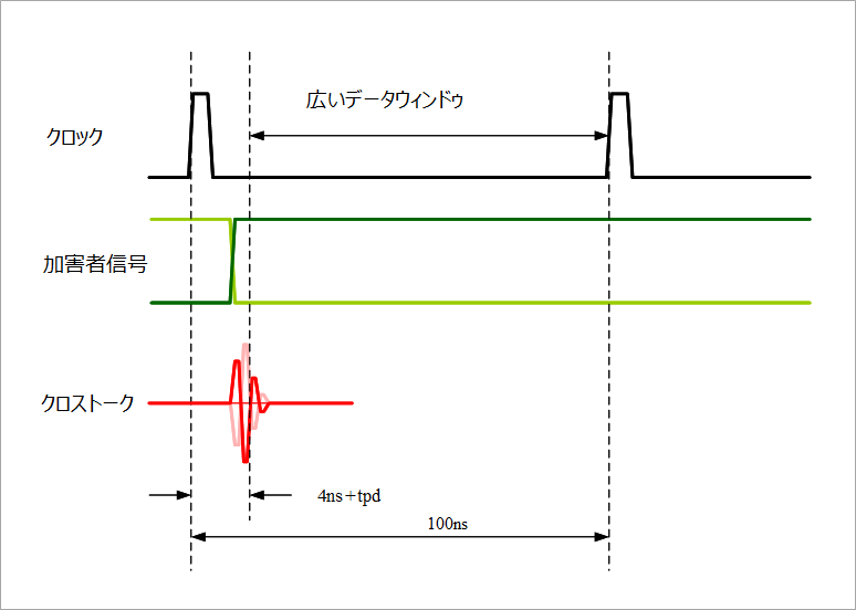
例えば、図1 のようなクロック周波数が 10MHz の TTL の場合のクロストークを考えます。設計が悪くて 2番目の山(谷)までクリアする必要があるとします。配線長を 15cm とすると、信号が片道に要する時間は、τ=1ns です。図1 のクロストークのパルス幅は 2τ=2ns となります。したがって、ウィンドウは 100ns に対して 4ns 狭くなります。
100ns-4ns、すなわち、96ns に対して、それぞれ数 ns のセットアップ/ホールド時間を考えるので、広いデータウィンドゥがあります。(実際には加害者信号の遅延時間を考慮する必要があります。)クロックがこの 5倍の 50MHz になっても、周期は 20ns なので、まだかなりの余裕がありました。
ただし、TTL が遅くて CMOS が速いというわけではありません。(脚注)
高速の CMOS
クロック周波数を 500MHz とすると周期は 2ns です。配線長を 4cm (τ=0.25ns) としても上記のように 2番目の谷(山)まで考えると 4τ=1ns なので、そんな余裕はありません。やむを得ない場合にでも最初の山(谷)が収まるまで 2τ=0.5ns 待ちます。2ns の周期に対して 0.5ns は辛いので、クロストークノイズでノイズマージンを超えることは避ける必要があります。
一方で、シグナルインテグリティへの理解が深まり、反射やクロストークを低減する設計が行われるようになりました。したがって、振幅軸上で誤動作することはかなり少なくなりました。
ノイズマージンからタイミングマージンへ
振幅上の誤動作が減少する一方、高速化により、振幅軸から時間軸への関心が高くなってきました。
「ノイズマージンの考え方」で延べたように、ノイズマージンは、TTL 時代の 0.4V から 1.0V へ増加し、さらに、差動シングル入力を用いると、1.5V 程度まで増加しました。また、データシートには明確には記載していませんが、スレッショールド電圧の不確定さはタイミングマージンを削っています。
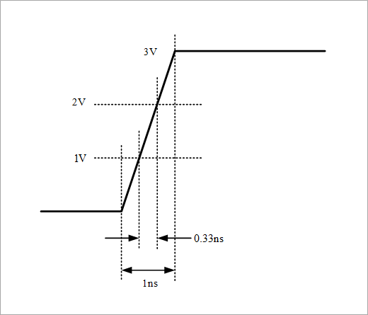
例えば、図2 のように、信号の立ち上がり時間が 1ns (0-100%) のとき、スレッショールド電圧の不確定さを 1V/2V とすると、タイミングの不確定さは 0.33ns となります。クロック周波数を 500MHz とすると、0.33ns は、周期 2ns に対して 16% となり無視できません。差動シングル入力を用いると、この時間軸上の不確定さを回避できます。
信号の変化時のノイズ重畳
ノイズ低減の設計やスレッショールドの不確定さを回避する素子などによりノイズの問題はかなり改善されました。ノイズは、従来のように "0"、"1" のロジック信号に重畳するだけではなく、過渡時に重畳することにより新たな問題が顕在化してきました。
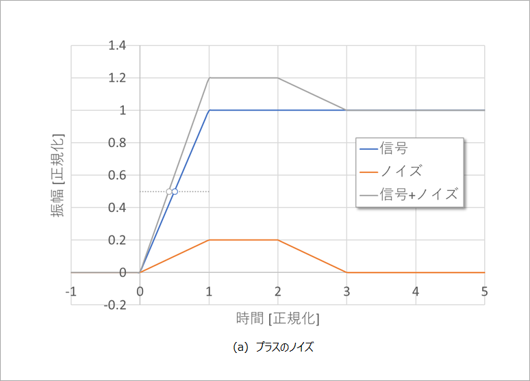
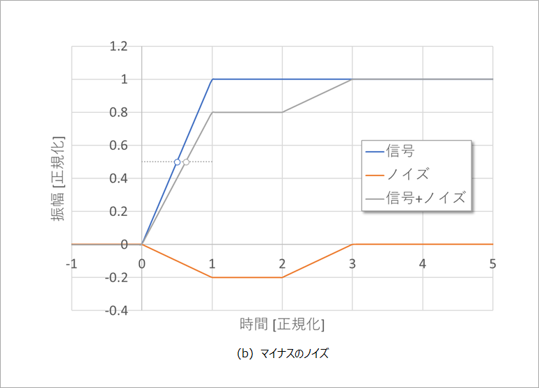
図3 に示すように、信号の立ち上がり付近にノイズが重畳するとスレッショールドの位置がずれます。立ち上がりに対して、プラスのノイズなら時間が早くなり、マイナスなら遅くなります。図3 は、立ち上がり時間と振幅をそれぞれ1に正規化しています。時間を ns で、振幅をボルトで考えると具体的ないイメージがつかめると思います。
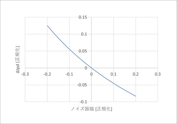
図4 は、図3 の条件で、ノイズの振幅を変化させたときの遅延時間の変化を示します。ほぼ振幅に比例します。
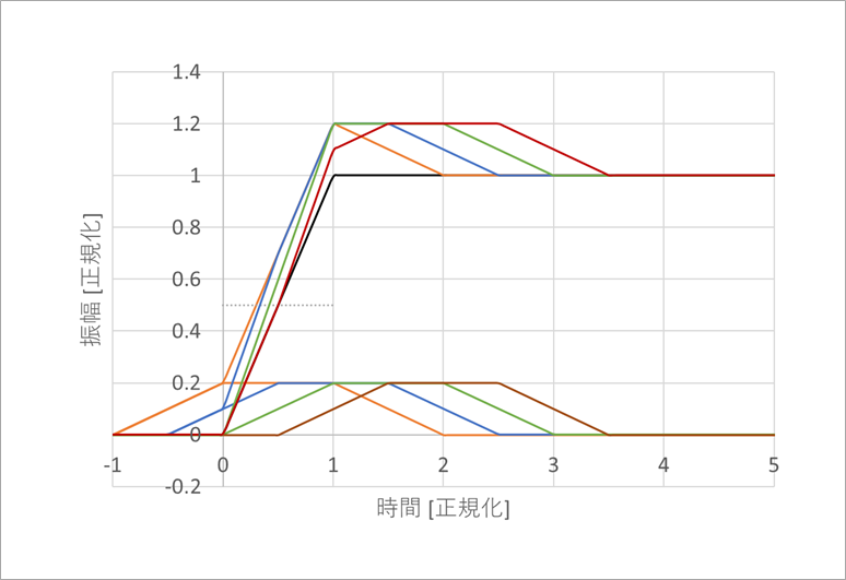
図5 は、ノイズの開始位置による波形の変化を、図6 には、発生位置と遅延時間の変化を示します。当然、波形の立ち上がりにノイズのピーク位置が一致したときに遅延時間の変化は最大となります。図5 および 図6 はプラスのノイズですが、マイナスのノイズに対しても同様です。
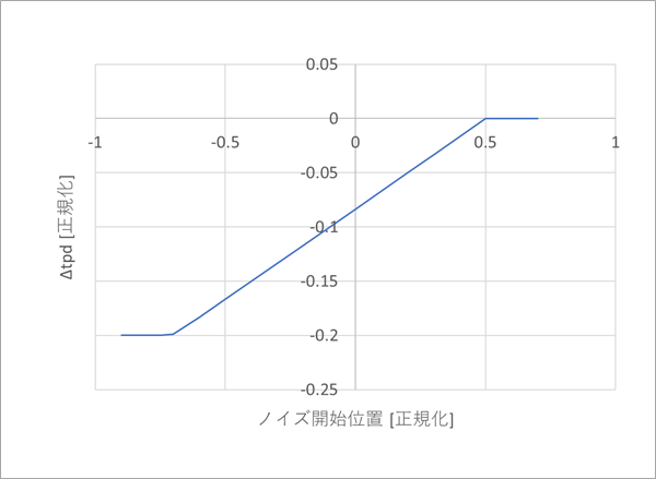
被害者信号のタイミングとノイズの位置が特定できればそのタイミングでタイミング設計を行いますが、特定できない場合は、最大のノイズが生じると考えて設計する必要があります。
この考え方は、ギガビット伝送の場合にジッタとして考慮する必要があります。微小なノイズでも、タイミングジッタとして現れるので、アイを狭めます。設計マージンは、振幅軸から時間軸へと移ったといっても過言ではないでしょう。
(脚注)
TTL 全盛のころの CMOS は、4000 シリーズでした。TTL ゲートの遅延時間の 10ns に対し、CMOS は 100ns、あるいはそれ以上で、CMOS は限られた用途、例えば、低消費電力や広い電源電圧向けに使用されていました。
TTL は、その後、74S や 74AS シリーズが次々に登場し、低電力向けには 74LS シリーズと、広い用途向けに多くのシリーズが発表されました。その後、CMOSは、メタルゲートからシリコンゲート(自己整合ゲートの実現)へと発展したことにより、高速・高集積化が実現し、TTL から主役の座を奪ったと考えます。
碓井有三のスペシャリストコラムとは?
基礎の基礎といったレベルから入って、いまさら聞けないようなテーマや初心者向けのテーマ、さらには少し高級なレベルまでを含め、できる限り分かりやすく噛み砕いて述べている連載コラムです。
もしかしたら、他にも気になるテーマがあるかも知れませんよ!