- Semiconductor BusinessHOME
- Products and Services of Macnica,Inc.
-
technical information

-
Events and Seminars
- Handling Manufacturer
- Support
- Inquiry
- Click here to purchase products
- Semiconductor business e-mail magazine registration
![]()
![]() Narrow down by specifying conditions
Narrow down by specifying conditions
現在2168件がヒットしています。check
VIH is the voltage at which input voltage above this value is recognized as high when it exceeds this value, and VIL is the voltage at which input voltage below this value is recognized as low when it falls below this value. It goes without saying that VOH and VOL represent the high and low output voltage levels.
Logic IC characteristics
Most logic ICs are CMOS nowadays, but they were TTL before CMOS. Since the meaning and positioning of VOH and VOL in the output voltage are different between CMOS and TTL, some CMOS generation people may wonder why these values are specified.
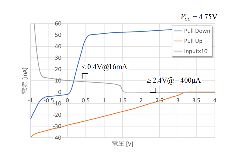
Figures 1 and 2 show the TTL and CMOS input and output static characteristics. Figure 1 is the first generation 7400 and Figure 2 is the CMOS input/output characteristics of a typical 16mA driver. In Figures 1 and 2, Pull Down is the low side characteristic and Pull Up is the high side characteristic. In general, these properties can be obtained from ibis, but since ibis had not yet appeared in the TTL era, ibis for TTL is not available. (New series 74F and 74AS are available.)
The details of the input characteristics will be described later, but 10 TTL characteristics are shown in Figure 1. Since CMOS has almost zero input current, it is superimposed on the horizontal axis. (The thick horizontal axis shows a straight line where the current is almost zero.)
Input/Output level
The input/output levels determined in the TTL era were as below,
- VIH/VIL=2.0V/0.8V
- VOH/VOL=2.4V/0.4V
both have a margin of 0.4V. This 0.4V is the DC margin, and noise such as ground noise, power supply noise, and crosstalk noise is taken into consideration, which is, the noise budget is will be set.
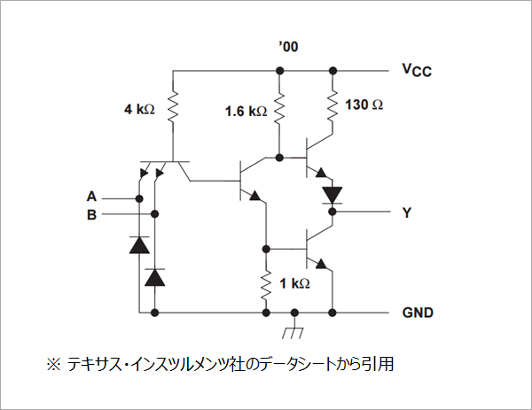
Figure 3 is a schematic of the SN7400, the most basic NAND gate in the SN74 series. When the previous stage is low, the input draws 4kΩ from VCC and through the base-emitter to the output of the previous stage. This current is IIL≧-1.6mA@0.4V (absolute value less than 1.6mA). So if 10 inputs are connected to one output, 16mA will flow into the output.
The TTL statics in Figure 1 shows the statics for 10 inputs. In other words, in the low side characteristics, VOL is 0.4V or less when 16mA is applied. This is said to have an input fan-in of 1 and an output fan-out of 10.
TTL VIH and VIL are 2.0V and 0.8V. This value is obtained from the schematic shown in Figure 3.
TTL output voltage
TTLs
| conditions | VCC | min | typ | max | unit | |
| VOL | IOL = 16mA | 4.75V | 0.2 | 0.4 | V | |
| VOH | IOH =-400uA | 2.4 | 3.4 | V |
CMOS
| conditions | VCC | min | typ | max | unit | |
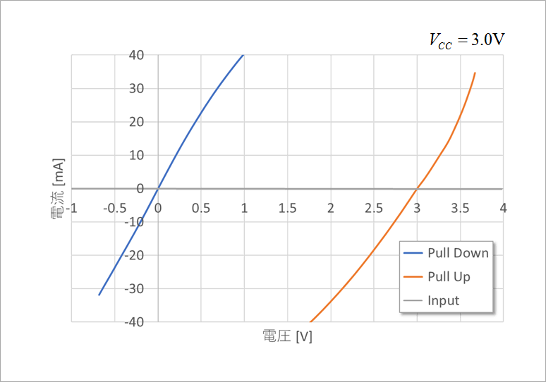
| VOL | IOL = 16mA | 3.0V | 0.25 | 0.4 | V | |
| VOH | IOH =-16mA | 2.6 | 3.05 | V |
Table 1 TTL and CMOS output voltages
Table 1 shows the TTL and CMOS output voltage specifications. For TTL, there was almost one type (footnote 1) standardized, but for CMOS, there are large variations in power supply voltage and output current, so this is the standard I arbitrarily decided. CMOS power supply voltages come in wide variations, such as 5V, 3.3V, 2.5V, and 1.8V, and output currents range from less than 1mA to around 24mA.
In both cases, the minimum value of the operating conditions is used for the power supply voltage when specifying the output voltage. That is, if VCC=5V specification, -5% VCC=4.75V, and if VCC=3.3V, specify VCC=3.0V.
In addition, the power supply voltage of bipolar ICs such as TTL is often referred to as VCC, and in the case of CMOS, it is often referred to as VDD. It seems to be used properly. In the past, for example, there were cases where the voltage supplied to the base was VBB, and the voltage supplied to the emitter was VEE, etc. However, since current logic ICs have a single power supply, I believe that there is no need to distinguish between VCC and VDD. I'm here.
TTL has been the industry standard for over 20 years, with the 74 series introduced by TI (Texas Instruments) in the 1960s. Logic was mainly composed by combining multiple basic gates such as NAND. Thus the output of one gate is connected to the input of the next gate. There was a limit to this number, and in the case of the SN74 series ICs, a maximum of 10 was fixed.
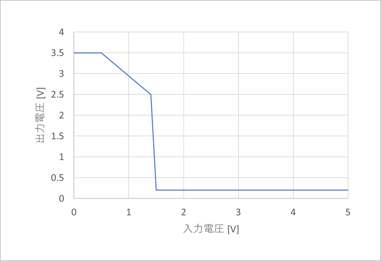
On the high side, the current of the input 1 terminal is 40uA, so 10 pieces is 400uA. Compared to the output characteristics on the high side, there is considerable margin. However, as the TTL input/output transfer characteristics are shown in Figure 4, where you should pay attention to is, when the input voltage VIL reaches the maximum value of 0.8V, the output voltage VOH will drop.
CMOS output voltage
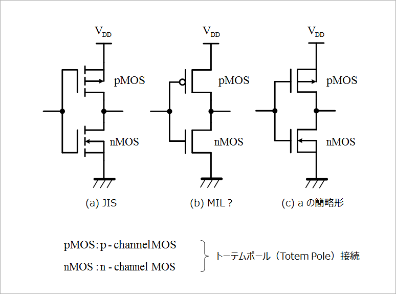
Figure 5 is a CMOS schematic. It is a p-channel MOS (pMOS) and an n-channel MOS (nMOS) stacked on top of each other. It is called a totem pole circuit because it resembles a carved totem pole used by Native Americans. The input threshold voltage of CMOS is determined by the tug-of-war between the threshold voltages of pMOS and nMOS, so it cannot be obtained from the circuit diagram. Generally, the CMOS threshold voltage is said to be 30-70% of the power supply voltage. For 3.3V voltage, VIL=1V and VIH=2V.
In the case of CMOS, the input current is almost zero, so no matter how many devices are connected, the DC output voltage will not change. Also, it is not common to connect more than one.
So let's think about what we mean by a 16mA driver. As I said earlier, TTL was used to build logic. At that time, the rise time of the output voltage was slow, and reflection was not usually considered. When logic ICs switched from TTL to CMOS, it was almost impossible to create logic with individual ICs, and one-to-one transmission made the rise time faster, so reflections when connecting ICs should be taken into consideration. A need has arisen. When analyzing this reflection, the drive capability of the output is required.
Looking at Figure 2, the characteristics are almost linear on both the low side (Pull Down) and the high side (Pull Up). Looking at the standard in Table 1, since it is 0.4V at 16mA, the slope of the output characteristics (reciprocal) is 400mV/16mA=25Ω, but this 400mV is the worst value including the manufacturing process and temperature. A typical characteristic is 16Ω at about 1/1.5 of this.
From Figure 1, the TTL no-load VOH and VOL are around 3.2V and 0.1V. On the other hand, from Figure 2, the CMOS no-load VOH and VOL are 3.0V and 0V, which is the full supply voltage. In analog, it's called rail-to-rail. In the case of CMOS, we often see VOL other than 0.4V. As mentioned above, the value of 0.4V itself has no meaning (footnote 2), and it has a strong meaning of specifying the output resistance, so 0.2V or 0.5V is fine. If the resistance derived from the voltage and current is very large, the nonlinear region of the output characteristic may enter the operating range, so care must be taken in analyzing reflections. Use Bergeron analysis if necessary.
Using ibis
Variations such as 74L, 74H, 74LS, 74S, 74F, 74AS, and 74ALS were born for the 74 series standards, and the standards themselves (mainly IOL and IOH) are also different.
Footnote 2
It made sense when mixing TTL and CMOS.
What is Yuzo Usui's Specialist Column?
It is a series of columns that start from the basics, include themes that you can't hear anymore, themes for beginners, and also a slightly advanced level, all will be described in as easy-to-understand terms as possible.
Maybe there are other themes that interest you!