- Semiconductor BusinessHOME
- Products and Services of Macnica,Inc.
-
technical information

-
Events and Seminars
- Handling Manufacturer
- Support
- Inquiry
- Click here to purchase products
- Semiconductor business e-mail magazine registration
![]()
![]() Narrow down by specifying conditions
Narrow down by specifying conditions
現在2189件がヒットしています。check
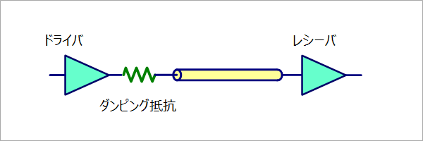
In signal transmission, it is common to connect drivers and receivers one-to-one, as shown in Figure 1. In this case, waveform distortion can be avoided by appropriately selecting the drive capacity of the driver or using the optimum damping resistance.
For damping resistance, please refer to "How to determine the value of damping resistance?"” and “Easier determination of damping resistor value”.
Many wires branch signals instead of one-to-one. This signal split is the most troublesome in terms of signal integrity.
Signal branches are classified as follows.
(1) Distributing the same signal to multiple locations
(2) Bus connection (memory module)
(3) Unintended branch
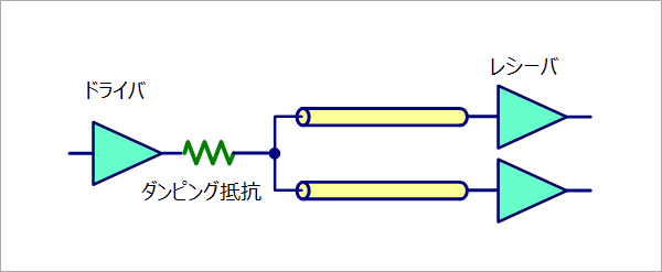
Example of (1)-1 Branching from the middle of wiring
Fig. 2 shows an example in which a signal is sent from the driver through one line and split into two along the way. Figure 3 is the equivalent circuit of the circuit in Figure 2.
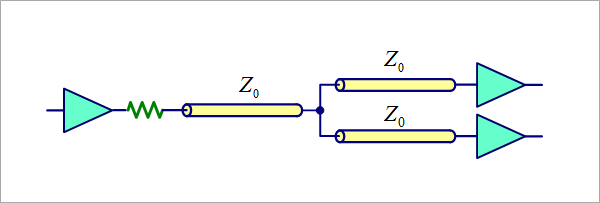
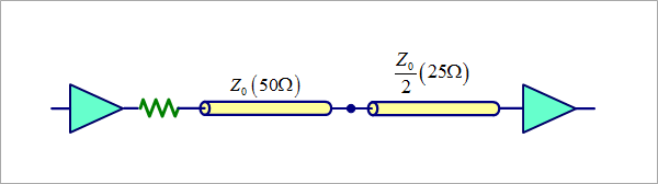
Since the two lines are connected in parallel, the parallel-connected part is equivalent to halving the characteristic impedance. If the characteristic impedance of the line is Z0=50Ω, reflection will occur at the point where it changes from 50Ω to 25Ω. The reflection coefficient at this connection point is (25-50)/(25+50)=-1/3, so it's a fairly large reflection.
For the reflection coefficient, please refer to "Trivia: Reflection Coefficient".
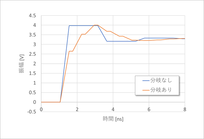
Figure 4 shows the far-end waveforms without and with a branch. This level of waveform disturbance seems to be within an acceptable range.
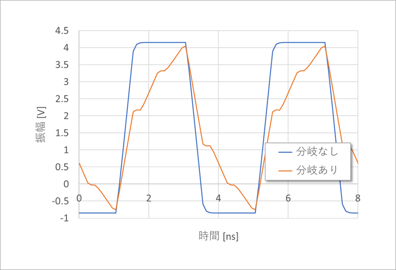
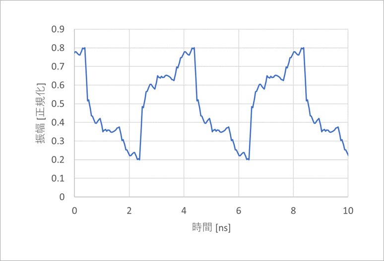
Figure 4 shows the response of a so-called step waveform where the signal changes from low to high. However, in practice, the pulse width is often narrow. For example, in the case of a repetitive waveform with 2 ns low and 2 ns high, it will look like Figure 5, and the rising stage will approach the threshold, so be careful. Is required. If you change the pulse width or period, the repetitive waveform will also change.
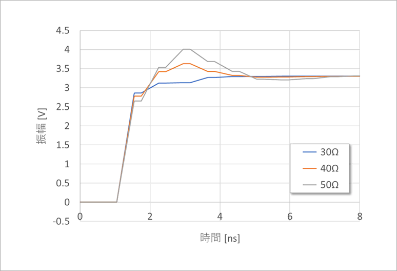
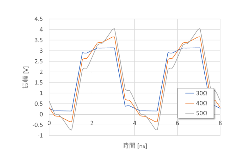
In this form, if you want to reduce reflection as much as possible, widen the pattern width of the line on the driver side and lower the characteristic impedance. Figure 6 is the step response and Figure 7 is the repetitive waveform. Both figures are examples of 30Ω to 50Ω on the driver side and two 50Ω branches on the other side. At 30 Ω, both step waveforms and repetitive waveforms have almost no waveform disturbance.
Ideally, the output should be 1:2 from the output of the driver, as shown in Figure 8, without branching in the middle. The drive capacity of the driver, including the damping resistance, should be chosen larger than the one-to-one ratio.
For example, adding an 18Ω damping resistor to a 12mA driver in a 1:1 transmission with a characteristic impedance of 50Ω will result in an overshoot of 10%. For how to find the damping resistance, please refer to "Damping resistance value determined more easily".
In the case of Figure 8, set the damping resistance to 0 (zero). The output resistance of the 12mA driver is 22Ω, and the characteristic impedance is 25Ω when two 50Ω wires are connected in parallel, so the overshoot is about 6%.
The wiring length after branching (strictly speaking, the delay time footnote 1) must be the same regardless of whether it is branched from the middle or branched from the output of the driver. This is the so-called equal-length (strictly equal-delay) wiring.
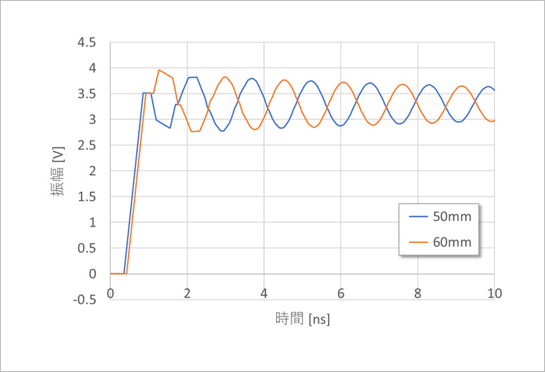
Figure 9 shows waveforms when the equal delay in Figure 8 is not observed. This is for two lines with lengths of 50mm and 60mm. Multiple reflections are repeated and the reflections never converge.
Example of (1)-2 Clock signal distribution
As shown in Fig. 10, if a certain amount of waveform distortion is allowed, a stepwise distribution method, such as 1:2, 2:4, and 4:8, has long been used. If it is rotated 90 degrees clockwise, it will look like a high school baseball tournament, so it is called a tournament system. The clock distribution of memory up to DDR2 is also this method.
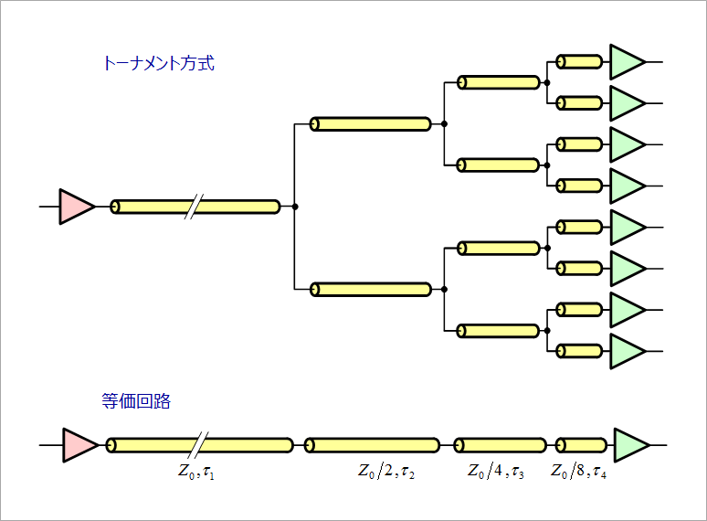
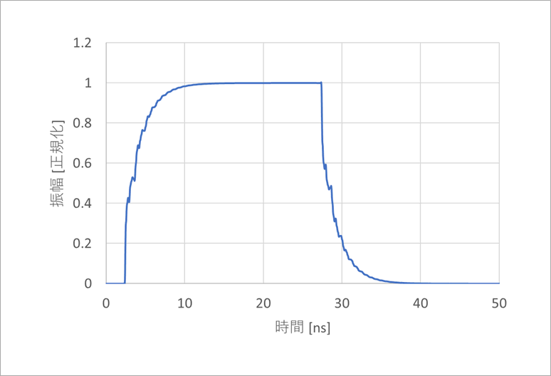
In addition, this clock distribution is used because reflection is generally not taken into consideration inside the LSI. In Example-1, the characteristic impedance changed from 50Ω to 25Ω due to parallel connection, but when branched into three stages, it equivalently changes to 50Ω, 25Ω, 12.5Ω, and 6.25Ω, so the waveform is greatly disturbed. . Figure 11 is for a wide pulse width and Figure 12 is for a narrow pulse width. Amplitude cannot be secured due to repeated reflections.
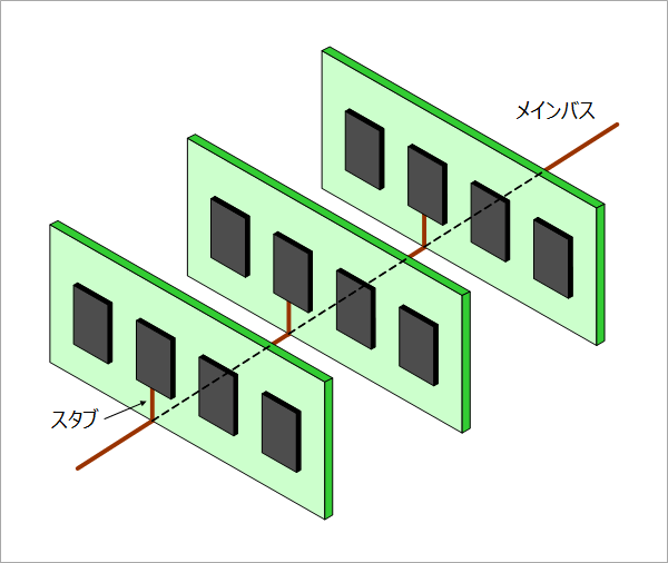
(2) Bus connection (memory module)
As shown in Figure 13, the memory module connects the bus wiring on the mother port to the memory element on the memory module with a short wiring. This connection repeats multiple reflections with the connection to the memory acting as a stub. To avoid this reflection, insert a resistor at the connection between the bus wiring and the stub. This method is called Stub Series Termination Logic (SSTL). For details, please refer to "Bits of Knowledge: SSTL - Part 1" and "Bits of Knowledge: SSTL - Part 2".
(3) Unintended branch
It is a branch that the designer is not aware of as a branch.
for example," What is a terminating resistor? ~ Part 3] is an example when a terminating resistor is connected as shown in Fig. 1. Termination resistors should be connected at the farthest end, but if the IC package size is large, the wiring from the termination location to the input of the farthest die becomes a stub. Please refer to the column above for solutions.
As IC packages became larger, it became difficult to observe the waveforms of IC pins, especially in the case of BGA. Therefore, from the middle of the pattern to be observed, as shown in Fig. 14, the wiring is pulled out to provide an observation pad.
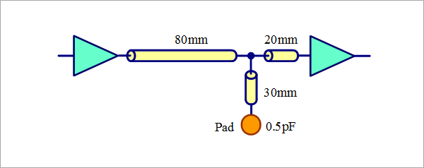
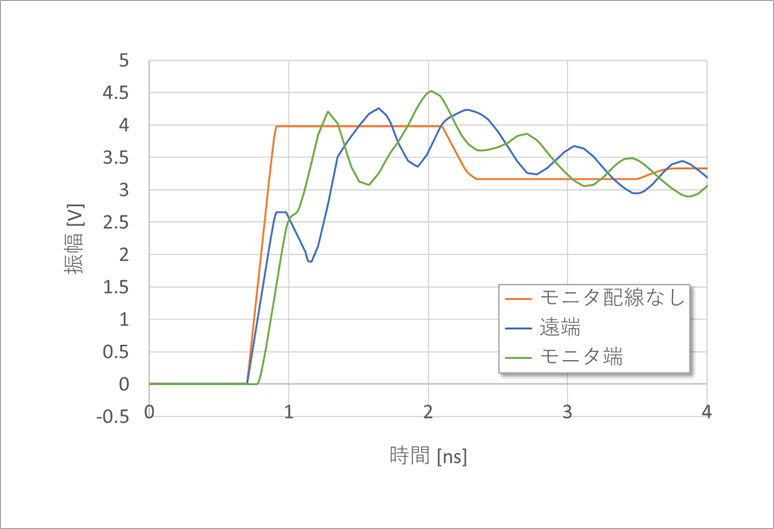
Figure 15 shows the effect of this observation wiring. In order to make the effect visible, the rise time of the signal was set to 200ps, and the wiring for this observation was set to 3cm long, but in the case of high-speed signals, it is necessary to avoid adding extra wiring for observation. . Please use the simulation together if necessary.
Footnote 1
The pattern delay time of the printed wiring board is different between the surface layer and the intermediate layer. The surface layer is about 6.5ns/m, and the intermediate layer is about 7.3ns/m.
What is Yuzo Usui's Specialist Column?
It is a series of columns that start from the basics, include themes that you can't hear anymore, themes for beginners, and also a slightly advanced level, all will be described in as easy-to-understand terms as possible.
Maybe there are other themes that interest you!