- 半導体事業HOME
- マクニカの製品・サービス
-
技術情報

-
イベント・セミナー
- 取扱メーカー
- サポート
- お問い合わせ
- 製品購入はこちら
- 半導体事業のメルマガ登録
![]()
![]() 条件を指定して絞り込む
条件を指定して絞り込む
現在2158件がヒットしています。check
DC/DCコンバーターのスイッチング周波数は、高くすべきか低く抑えるべきか悩んだことはありませんか?
少し前は300~500KHzが主流でしたが、最近は1~2MHzのスイッチング周波数の製品が一般的になってきて、なかには4MHz以上の製品まであります。
今回の記事は、この議論についての最終章になります。 過去2回にわたって、高い周波数のDC/DCコンバーターを用いた場合のメリットや注意点について説明させて頂きました。
第一章:高い周波数のDC/DCコンバーター使用した場合のメリット
第二章:周辺部品同士を接続する配線の寄生インダクタンスの影響
今回の記事では、PCB レイアウト上の寄生インダクタンスの影響をパワーグランド(P-GND)とシグナルグランド(S-GND)にフォーカスして確認した内容について説明させていただきます。
回路図は理想的GNDで書かれている
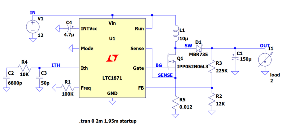
図1は、スイッチングレギュレーターLTC1871非同期式昇圧コンバーターです。 この回路図は、寄生インダクタンスを含まない理想的な回路となっています。
シミュレーションでは、LTC1871のGNDも外付けのコンポーネントのGNDも理想的な同電位にすることができます。しかし、実際には、各コンポーネントやPCBの寄生インダクタンスなどがありGND電位がずれます。実際にPCBのレイアウトのみにフォーカスしてGND回路を再現してみます。
パワーグランド(P-GND)とシグナルグランド(S-GND)
電源回路には、パワーグランド(P-GND)とシグナルグランド(S-GND)があります。これらのGNDを安定・強化することにより、ゲートの駆動のスイッチング電流の影響により、アナログコントローラー部に影響を与えないようする必要があります。通常、電源回路は単一の基板上にあり、すべてのグランドは同じ電位であることが理想です。ただし、P-GNDおよびS-GNDピンのいずれかがバウンスしている場合、電源回路のコントローラー部が影響を受ける可能性があります。
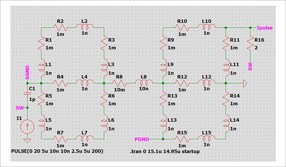
図2は、P-GNDおよびS-GNDを1mΩの抵抗と1nHのインダクタンスでメッシュ構成し、R8とL8で分割しているGNDパターンとしています。通常P-GNDとS-GNDは小さくて細い配線かスルーホールまたは0オームの抵抗器によって接続されています。ここでは、はんだの接続性や寄生インダクタンスがあった場合を考え、R8、L8で接続し影響を確認します。
寄生インダクタンスの影響
さて、このR8やL8の抵抗成分や寄生インダクタンスがあった場合、レギュレーターの動作に問題になるのでしょうか。シミュレーション結果を見てみましょう。
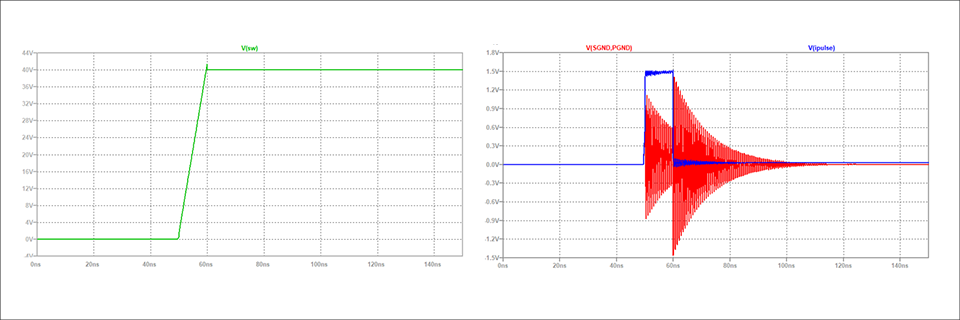
図3のスイッチノードの立ち上がり時間は、10nsと非常に速いです(図3のグリーンの波形)。この時、SWノードとS-GNDまでが1pFの小さな寄生容量としシミュレーションを実行した結果を確認すると、S-GNDノード(図3の赤色の波形/P-GND基準)で大きな電圧スパイクとリンギングが発生していることが確認できます。これにより、電源回路のコントローラー部分に電圧差が生じ、回路動作の問題が発生する可能性があることが確認できます。
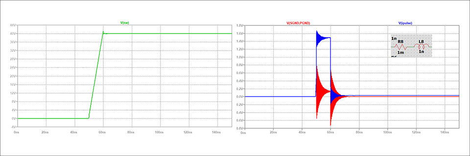
2つのS-GND間のリンギングを最小限に抑えるためには、P-GNDと接続している寄生インダクタンスL8を1mHから1nH、インピーダンスR8を10mΩから1mΩに小さくすることで改善することが推測できますので、シミュレーションで確認してみます。
P-GNDとS-GND関の寄生インダクタンスと抵抗を小さくする
実際にP-GNDとS-GND間のR8とL8の値を下げてみました。これにより、S-GNDのリンギングが小さくなったことが確認できます(図3の赤色の波形に対して図4の赤色の波形が小さくなっている)。
以上のことより、回路全体のシミュレーションでは現実世界の波形そのものを再現できるわけではありませんが、特定の回路部分(今回はGND)を設計される際に問題となる部分にフォーカスした形でシミュレーション回路を組むことで、デバイスやコンポーネントの配置、GNDの取り方などについて問題点を分かりやすく再現させることが可能で、注意すべき点について理解して頂けると思います。
コントローラータイプ別のPCBレイアウトの注意点
次に、他のタイプのコントローラーのPCBレイアウトを見ていきます。
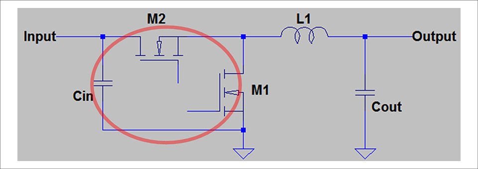
下記に、最も一般的なBUCKコンバーターの電力段を示します(図5)。この図でわかるように、制御MOSFETが上部にあることを除いてBUCKコンバーターは、BOOSTコンバーターと同じように見えます。 これにより、入力側でパルス化されたスイッチング電流が発生します。 この場合、高いスイッチング電流を処理する必要があるのは入力コンデンサーで、赤丸部分のループを小さくする必要があります。 出力コンデンサーには、小さなのこぎり歯状のリップル電流しか流れません。
パルス状のグランド電流は、MOSFET M1と入力コンデンサーから発生します。M1と入力コンデンサーを隣り合わせに配置すると、2つの電流が加算されます。 結果として生じる接地電流は、のこぎり歯状の電流リップルが重畳されたDC 電流のようになります。残りのコンポーネント配置とPCBレイアウトは、BOOSTコンバーターのPCBレイアウトとまったく同じです
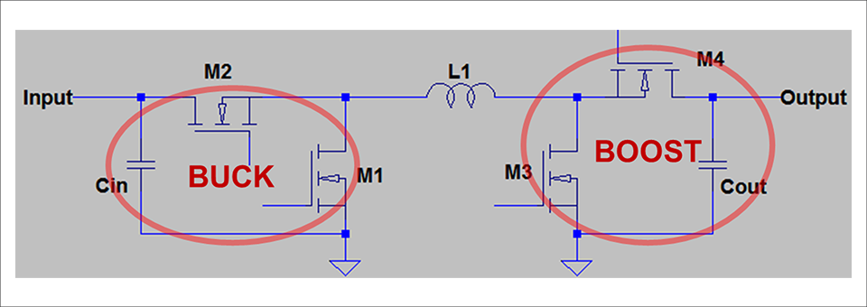
次にBUCK-BOOSTコンバーターの場合を考えます。回路を下記に示します。
一見すると、BUCK-BOOSTコンバータはより複雑です。ただし、回路はBUCKコンバーターとBOOSTコンバーターに分解できます。各回路は入力電圧に応じて動作が切り替わります。
入力電圧が出力電圧よりも低い場合は、BOOSTコンバーターとして動作し、入力電圧が出力電圧より高い場合、BUCKコンバーターとして動作します。この回路の各セクションは、個別にレイアウトできます。
2つのセクションは互いに接近している必要はありません。ただし、EMIの発生源であるスイッチノードのサイズを最小限に抑えるために、それらを近づけることをお勧めします。また、コントローラーを2つの高スイッチング電流領域に近づけないようにします。
また、Buck, Boost, Buck-Boostコンバーターの共通項となりますが、基本的にMOSFET/スイッチ・ノード~インダクター~出力コンデンサー(Cout)は、同一面に配置頂くことを推奨します。配置面が異なると配線距離が長くなりタイトなレイアウトが実現できず、スルーホールやビアを通すなどで対応した場合、その部分での寄生インダクタンスが発生し、スイッチング時に大きなスパイク電圧を発生させてしまう可能性があるので注意が必要です。
まとめ
レギュレーターにおける高いスイッチング周波数を取り扱うためのPCBレイアウト(1) ~ (3) では、高いスイッチング周波数、大電流電力コンバーターのPCBレイアウトを実装するための注意事項の一部を紹介しました。レギュレーターのレイアウトが良く分からない方は、ガイドラインとしてデモボードの PCB レイアウトを必ず参照してください。
また、PCB レイアウトの詳細を知りたい方は、「アプリケーション ノートAN-136」を参照してください。
おすすめセミナー/ワークショップはこちら
[オンラインセミナー] アナログソリューション 電源設計セミナー <無料>
おすすめ記事/資料はこちら
お問い合わせ
本記事に関して、ご質問などありましたら以下よりお問い合わせください。
アナログ・デバイセズ メーカー情報Topへ
アナログ・デバイセズ メーカー情報Topページへ戻りたい方は、以下をクリックください。