- Semiconductor BusinessHOME
- Products and Services of Macnica,Inc.
-
technical information

-
Events and Seminars
- Handling Manufacturer
- Support
- Inquiry
- Click here to purchase products
- Semiconductor business e-mail magazine registration
![]()
![]() Narrow down by specifying conditions
Narrow down by specifying conditions
現在2168件がヒットしています。check

Have you ever wondered whether the switching frequency of a DC/DC converter should be kept high or low?
Not long ago, 300 to 500 kHz was the mainstream, but recently products with a switching frequency of 1 to 2 MHz have become common, and there are even products with a switching frequency of 4MHz or higher.
When using a high-frequency DC/DC converter, the advantage of using a smaller inductor size was discussed in the previous article, "PCB layout for handling high switching frequencies in regulators (1)," using LTspice's ideal circuit. I hope you can understand the explanation.
In this article, we will use the LTC1871 step-up switching regulator simulation circuit that is actually on the market to check the switching waveforms and the effects of parasitic inductance on the PCB layout.
When a simulation is performed with an ideal model
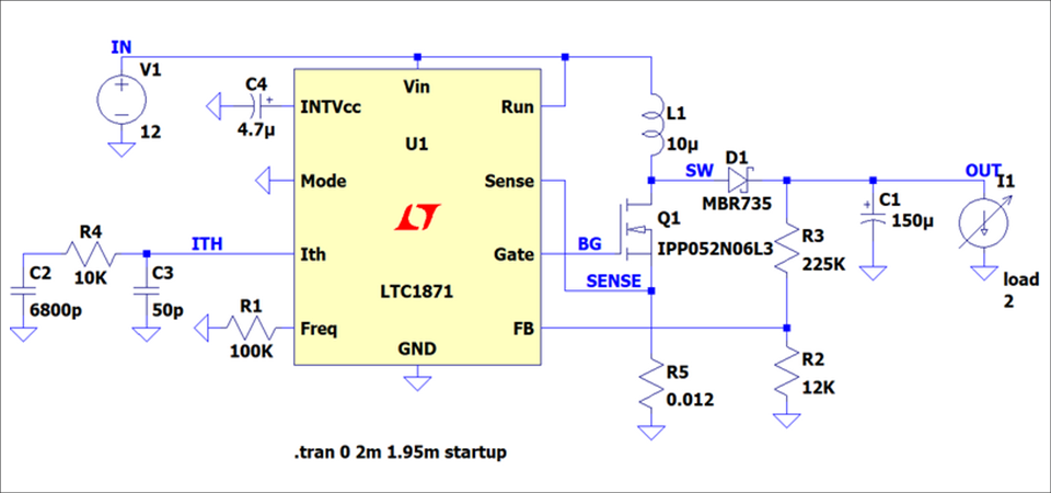
The switching regulator LTC1871 is a non-synchronous boost converter using an external MOSFET and Schottky diode at the output.
A SPICE model of the LTC1871 was usedto configure a boost converter with an input voltage of 12 (V), an output voltage of 24 (V), and a load current of 2 (A), as shown in Figure 1.
I would like to run the simulation and check the waveforms at each terminal.
Download the created LTspice file from the link below and run it.
simulation result
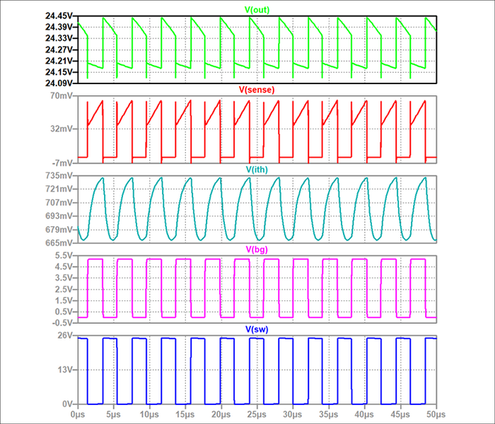
Figure 2 shows the simulation results. From the top, the output waveform, the SENSE pin waveform, the Ith pin waveform, the GATE (BG) pin waveform, and the switch (SW) node waveform.
Waveforms are stable. The signal on the control pin Ith is clean, with only normal rising edge spikes on the SENSE pin. Also, there are no voltage spikes on the switch node. Is this waveform the same as that of a real boost converter?
In reality, the waveform will be completely different from the simulated waveform. The switch node can overshoot and the GATE pin can undershoot, violating the GATE pin absolute maximum specification. Similarly, the switch node may undershoot and violate the absolute maximum ratings. These symptoms can occur in the real world and can be exacerbated by your PCB layout.
Considering board pattern parasitic inductance
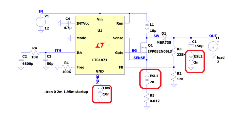
Now, an actual circuit has parasitic components such as parasitic inductance. Figure 3 shows a boost converter circuit with added parasitic inductance (framed in red). This circuit adds parasitic inductance to the GND pin of the controller. This is an important factor, which we will discuss below. Parasitic inductance other than the red frame is omitted because it is not important in this simulation.
Parasitic inductance comes from component geometry and PCB layout. Parasitic inductance in series with MOSFETs, diodes and output capacitors can be a problem due to very high current slew rates. A high current slew rate creates a large voltage across these parasitic inductances.
Effects of parasitic inductance
Now let's look at the simulation results.
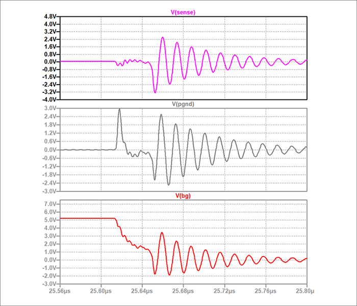
Check the output waveform affected by the inductance in Figure 4. There is a fair amount of high frequency ringing. There is a voltage spike on the Ith control pin of the first stage and the SENSE pin of the second stage. These voltage spikes can be very problematic as the controller can be affected.
Also, there is ringing on the P GND of the 3rd stage controller. This creates a voltage difference between the external component and the GND of the controller. The 4th stage GATE drive pin also has excessive ringing. Note that this ringing may exceed the maximum rating of the gate pin and cause failure.
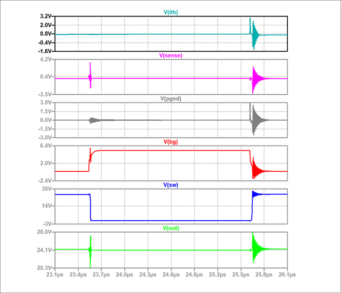
Let's zoom in on the waveform a little more.
Looking at the expanded output waveform in Figure 5, we can clearly see the problem with parasitic inductance. The number one problem is exceeding the maximum ratings of the controller pins. In particular, gate driver pins are subject to ringing and can cause circuit problems. To minimize these problems, parasitic inductance should be minimized.
The first point is to choose components with low parasitic inductance for power MOSFETs and output capacitors.
Packages for the external power MOSFET (IPP052N06L3) include TO-220 and TO-263 type packages. The TO-220 package has a single source pin approximately 13 mm long. The TO-263 type package has a source pin that is approximately 4 mm long. Considering only the length, the TO-220 package can be considered to have a parasitic inductance more than three times larger than the TO-263 type.
To minimize the inductance of the output capacitor, it is recommended to choose surface mount type ceramic capacitors instead of capacitors with lead terminals. Also, by connecting ceramic capacitors in parallel, the equivalent series inductance is greatly reduced.
Second, to reduce parasitic inductance, power MOSFETs, diodes, and output capacitors should be placed as close as possible and connected with thick, short wires. This becomes the most important layout convention.
Summary
In an ideal simulation, such as Figure 1, both the GND of the LTC1871 itself and the GND of external components can ideally be at the same potential. However, we found that the potential actually fluctuates due to the parasitic inductance on each component and PCB, as in the circuit shown in Fig. 3.
I hope you have understood from the simulation waveforms that the effects of these parasitic inductances can cause power supply IC malfunctions and failures.
The next article will be the final article, but I would like to conduct simulations using LTspice in a form that specializes in power grounds and signal grounds, and consider the effects and precautions of PCB layout.
Click here for recommended seminars/workshops
[Online Seminar] Analog Solution Power Supply Design Seminar <free>
[Online Seminar] Analog Solution Thermal Design Seminar <Free>
Click here for recommended articles/materials
Inquiry
If you have any questions regarding this article, please contact us below.
Analog Devices Manufacturer Information Top
To return to the Analog Devices manufacturer information top page, please click below.