- Semiconductor BusinessHOME
- Products and Services of Macnica,Inc.
-
technical information

-
Events and Seminars
- Handling Manufacturer
- Support
- Inquiry
- Click here to purchase products
- Semiconductor business e-mail magazine registration
![]()
![]() Narrow down by specifying conditions
Narrow down by specifying conditions
現在2184件がヒットしています。check

Precision operational amplifier ADHV4702-1 capable of direct 220V input
Applications such as high-side current sensing, high-voltage drivers, ATE (automated test equipment), and LiDAR require high-voltage analog circuits exceeding tens of volts.
High-voltage analog circuits have previously been achieved using discrete transistor circuits, but these have posed challenges such as the high cost of components, the difficulty of miniaturizing the circuits, and heat generation.
The ADHV4702-1 from Analog Devices is a high-voltage, high-precision operational amplifier that solves these challenges through the company's proprietary next-generation semiconductor process and innovative architecture.
This article introduces the following four features of the ADHV4702-1.
- Low noise measurement of high voltage signals with few parts
- Drives signal outputs up to 220V without expensive discrete transistor circuits
- Thermal protection with internal temperature sensor and shutdown function (thermal shutdown)
- Small package with EC61010-1 compliant pinout
Low noise measurement of high voltage signals with few parts
The ADHV4702-1 is designed using Analog Devices' proprietary next generation bipolar/complementary metal-oxide semiconductor (CMOS)/laterally diffused metal-oxide semiconductor (BCDMOS) process.
These technologies enable the ADHV4702-1 to realize high-voltage, high-precision analog circuits with a small number of components.
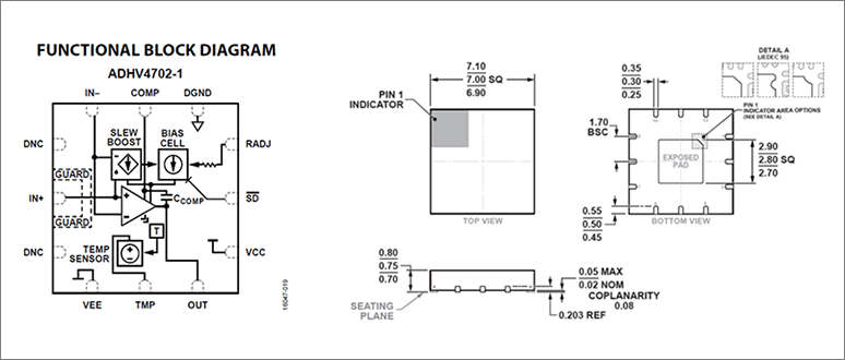
The functional block diagram of the ADHV4702-1 is shown below.
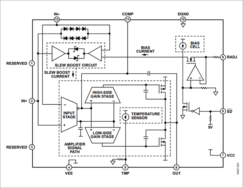
The ADHV4702-1 input stage architecture offers the benefits of low input bias current, low input offset voltage, low drift, and low noise with high input impedance for precision applications such as automatic test equipment (ATE).
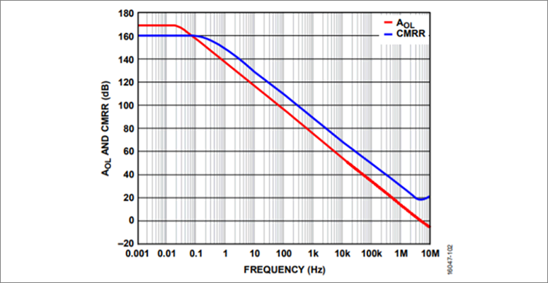
The ADHV7402-1 achieves precision performance with an open-loop gain (AOL) of 170 dB (typical) and a common-mode rejection ratio (CMRR) of 160 dB (typical), as shown in the performance graphs below. The ADHV4702-1 also achieves an input offset voltage (VOS) drift of 2 µV/ºC (maximum) and an input voltage noise of 8 nV/√Hz.
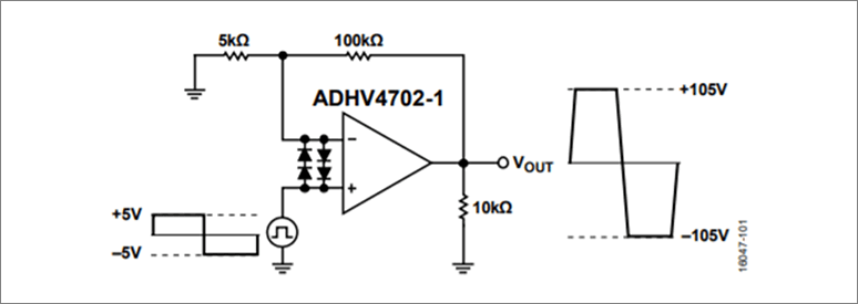
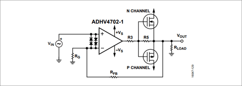
Drives signal outputs up to 220V without expensive discrete transistor circuits
The ADHV4702-1 operates from ±110 V symmetrical split supplies, asymmetric split supplies, or a 220 V single supply.
This wide supply voltage range enables high voltage circuits with few external components, as in the typical application circuit below.
The ADHV4702-1 can also realize the following functions depending on the peripheral circuit configuration.
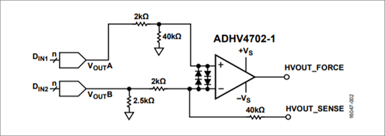
Voltage Subtractor with High Voltage DAC
In this configuration, the ADHV4702-1 is set up as a voltage subtractor with a gain of 20, making it ideal for bias control in chemical analysis (mass spectrometry), driving piezos, scanning electron microscopes (SEM), LiDAR APD/SPADs, silicon photomultipliers, and more.
high current output driver
By implementing a unity gain output stage using discrete components, the ADHV47021 can be used as a high power output driver.
The output current drive can be amplified to the currents that can be handled by discrete products while maintaining the precision performance of the amplifier alone, such as offset, drift, open-loop gain, and CMRR.
Thermal protection with internal temperature sensor and shutdown function (thermal shutdown)
Operating an IC at temperatures above its absolute maximum rating may affect product reliability.
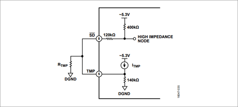
To minimize this risk, the ADHV4702-1 features a resistor adjustable thermal shutdown option.
The ADHV4702-1 is disabled and enters a low power state when the voltage on the SD pin drops to within 0.8 V of DGND, reducing the quiescent current to approximately 0.18 mA.
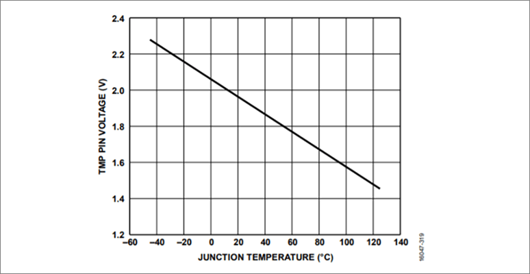
In addition, the temperature information output as a voltage to the TMP pin indicates the approximate temperature of the IC chip, so it can also be used to monitor power consumption. By performing a one-time calibration of the TMP pin at room temperature, the temperature can be measured more accurately.
The graph below shows the relationship between the TMP pin voltage and the junction temperature.
As shown in the following circuit diagram, the thermal shutdown function can be realized by connecting TMP and SD and connecting a 200kΩ resistor (RTMP) between TMP and SD and DGND as close as possible to the ADHV4702-1.
Small package with IEC61010-1 compliant pinout
The ADHV4702-1 has a package configuration that complies with IEC61010-1, a safety standard related to measuring instruments.
In addition, the package size is 7mm x 7mm (LFCSP), contributing to miniaturization and multi-channelization of circuits.
The main functions of ADHV4702-1 are as follows.
Wide operating voltage range
〇 Dual power supply operation: ±12V to ±110V
o Asymmetric power supply operation: 24V to 220V
Wide input common-mode voltage range: 3V from rails
High Common Mode Rejection Ratio: 160dB (Typical)
High AOL: 170dB (typical value)
●Fast slew rate
〇74V/μs (typical value)
〇24V/μs (typ.) when using external input clamp diode
Low input bias current: 2pA (maximum)
● Low input offset voltage: 1 mV (maximum) ●
Low input offset voltage drift: 2 μV/°C (maximum)
Low Input Voltage Noise: 8nV/√Hz (Typical) at 10kHz
Wide small-signal bandwidth: 10MHz (typical)
Resistor Adjustable Quiescent Current: 0.6mA to 3mA (VS = ±110V)
●Stable operation with unity gain
Thermal monitoring
Shutdown mode
Small footprint: IEC 61010-1 space compliant 12-pin, 7mm × 7mm LFCSP
Application example
- High side current sensing
- ATE (automatic test equipment)
- high voltage screwdriver
- piezo transducer
- Digital-to-Analog Converter (DAC) Output Buffer
- Bias in LiDAR

Click here for recommended articles/materials
Click here to purchase products
Inquiry
If you have any questions regarding this article, please contact us below.
Analog Devices Manufacturer Information Top
If you want to return to Analog Devices Manufacturer Information Top, please click the button below.