- Semiconductor BusinessHOME
- Products and Services of Macnica,Inc.
-
technical information

-
Events and Seminars
- Handling Manufacturer
- Support
- Inquiry
- Click here to purchase products
- Semiconductor business e-mail magazine registration
![]()
![]() Narrow down by specifying conditions
Narrow down by specifying conditions
現在2183件がヒットしています。check

Regardless of the application, there are common needs for precision data acquisition systems: miniaturization, reduction of peripheral components, and reduction of design effort while maintaining the performance of the current configuration. This article introduces Analog Devices' first modular AD converter, the ADAQ798x, which realizes these needs.
What is SiP design? Background of AD converter modularization
Many data acquisition applications are moving to an ADC-per-channel approach, and the drive to increase the number of channels without changing the form factor is accelerating. As a result, channel density is of great concern to many designers of data acquisition signal chains.
In addition, there is a growing demand to improve the usability of precision ICs and make it easier to achieve the performance specified in the datasheet.
In order to solve these problems, the number of cases where subsystems applying SiP (system in package) technology are being developed as IC products for the signal chain is increasing.
ADAQ798x series of first SiP devices from Analog Devices
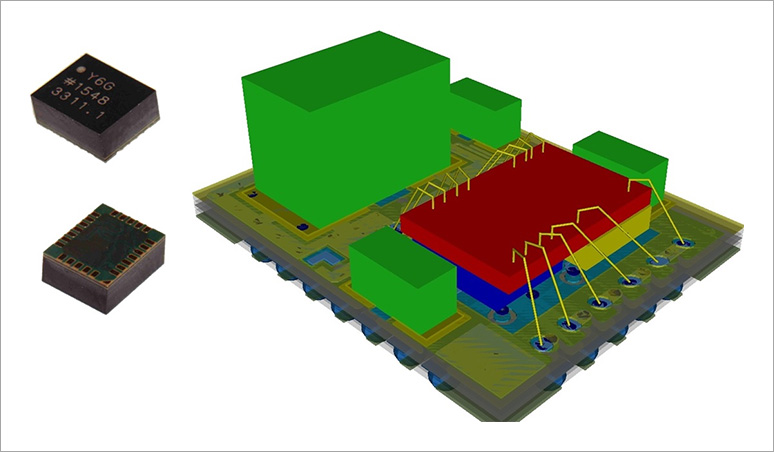
The first data acquisition device developed by Analog Devices, the ADAQ798x, is a 16-bit analog-to-digital converter (ADC) μModule® data acquisition system that integrates four common signal processing and conditioning blocks into a SiP design that addresses a wide range of applications.
These devices integrate the most critical passive components to overcome many of the design challenges associated with traditional signal chains that use successive approximation register (SAR) ADCs.
The built-in passive components are essential to achieving the specified device performance, and the fact that the performance of the device is guaranteed with the passive components included is a unique feature of modules and offers significant benefits to designers.
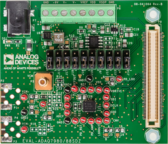
ADAQ798x Series Product Brief
The ADAQ798x combines a precision, low power 16-bit SAR ADC, a low power, wide bandwidth, high input impedance ADC driver, a stable, low power reference buffer, and an efficient power management block in a small 5 mm × 4 mm LGA package, simplifying the design process for data acquisition systems.
The ADAQ798x system-level integration solves many design challenges, providing a flexible ADC driver feedback loop that allows adjustable gain and common-mode, as well as single-supply operation with minimal impact on the device's operating specifications.
The ADAQ7980/ADAQ7988 integrate into small, integrated circuit (IC)-like form factors key components commonly used in data acquisition signal chain designs.
The μModule family shifts the design burden of component selection, optimization and layout from the designer to the device, reducing overall design time, system troubleshooting and ultimately improving time to market.
The SPI-compatible serial interface using the SDI input allows daisy-chaining of multiple devices on a single 3-wire bus and provides an optional busy indicator. The user interface is compatible with 1.8 V, 2.5 V, 3 V, or 5 V logic.
Features of ADAQ798x
- Easy to deploy
- μModule Data Acquisition Subsystem
- All active components are designed by Analog Devices
- 50% space savings
- Integrates critical passive components
- Serial interface: SPI/QSPI™/MICROWIRE™/DSP compatible
- Multiple ADAQ7980/ADAQ7988 can be daisy chained
- Supports various power supply configurations for 1.8 V/2.5 V/3 V/5 V logic interfaces
- μModule Data Acquisition Subsystem
- high performance
- 16-bit resolution with no missing codes
- Throughput: 1 MSPS (ADAQ7980), 500 KSPS (ADAQ7988)
- INL: ±8 ppm (typ.), 20 ppm (max.)
- SNR: 91.5 dB typical at 10 kHz (unity gain)
- THD: -105dB at 10kHz
- Zero error: ±0.06mV typ (typical) @ gain 1
- Zero error drift: 1.3μV/°C (max)
- Low power consumption
- 21mW typical at 1MSPS (ADAQ7980), 16.5mW typical at 500KSPS (ADAQ7988)
- Flexible power-down mode
- Tiny, 24-pin, 5 mm × 4 mm LGA package
- Excellent ESD rating
- Human Body Model (HBM): 3500 V
- Field-Induced Charged Device Model (FICDM): 1250 V
- Wide operating temperature range: -55°C to +125°C
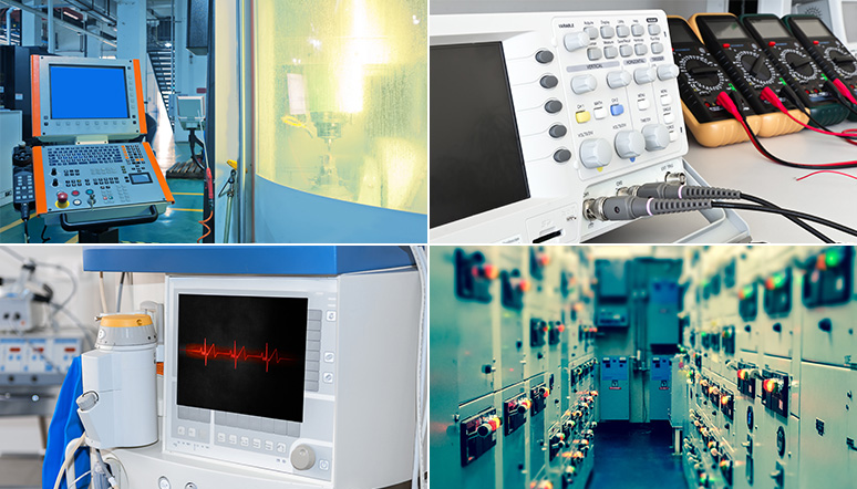
Application example
- Automatic Test Equipment (ATE)
- battery powered instrument
- communication
- data acquisition
- process control
- medical instruments
Click here for recommended articles/materials
Click here to purchase products
Inquiry
If you have any questions regarding this article, please contact us below.
Analog Devices Manufacturer Information Top
If you want to return to Analog Devices Manufacturer Information Top, please click the button below.