- Semiconductor BusinessHOME
- Products and Services of Macnica,Inc.
-
technical information

-
Events and Seminars
- Handling Manufacturer
- Support
- Inquiry
- Click here to purchase products
- Semiconductor business e-mail magazine registration
![]()
![]() Narrow down by specifying conditions
Narrow down by specifying conditions
現在2176件がヒットしています。check

When developing high-precision measuring equipment, operational amplifiers and AD converters that require both positive and negative power supplies are used. In such cases, the design of the positive and negative power supplies becomes an issue.
In this article, we will first touch on the issues that arise when designing positive and negative power supplies, and finally introduce a solution that can be configured simply and with low noise.
Problems of positive/negative power supply design (1)
The problem with designing a positive/negative power supply is that the power supply circuit becomes complicated.
Even when designing a simple step-down switching power supply circuit, it becomes complicated if you design it using discrete components, but designing an inverting negative power supply becomes even more complicated.
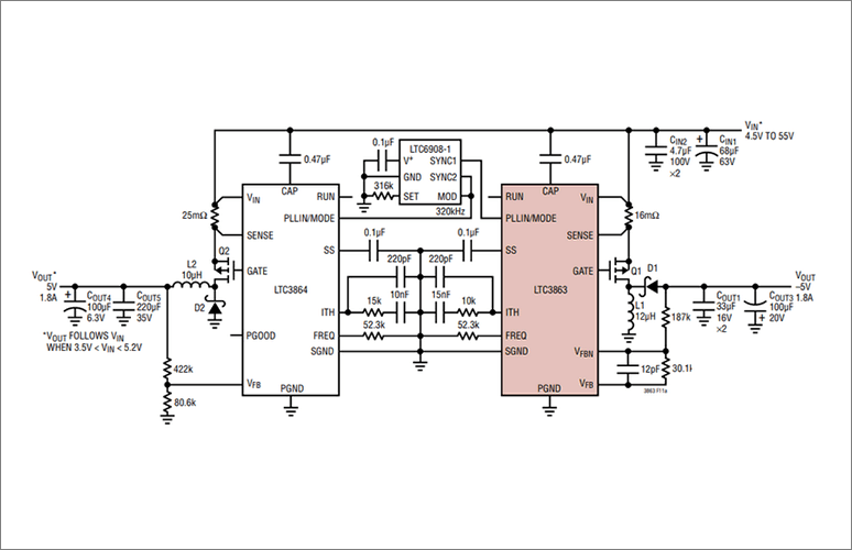
Figure 1 shows an example of a ±5V output power supply circuit for a switching power supply using the LTC3863 and LTC3864. Because it uses two switching regulators, the circuit scale is large, which can make pattern design difficult.
Problems of plus/minus power supply design (2)
The output of a switching regulator has a lot of noise and cannot be fed directly into an operational amplifier or AD converter, so two linear regulators are required for the circuit in Figure 1. This makes the circuit size even larger.
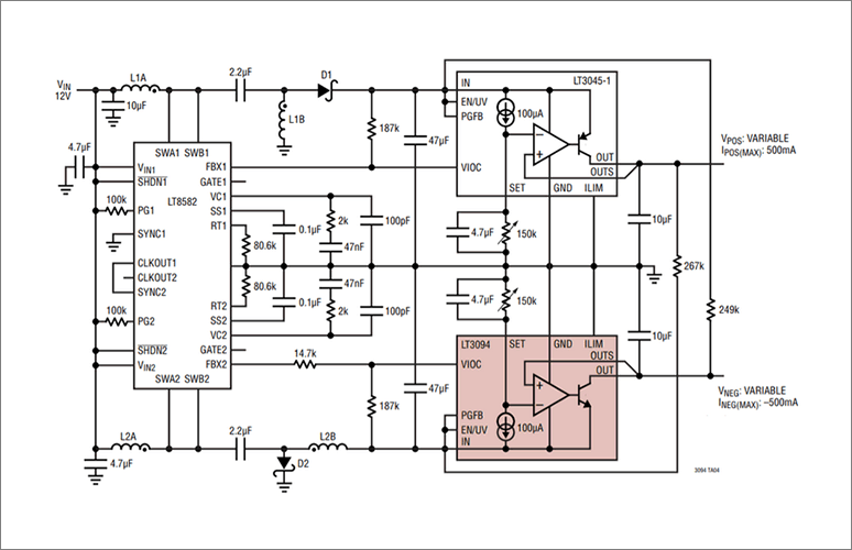
An example of a circuit that uses a single switching regulator to create a positive and negative power supply is shown in Figure 2. This is simpler than the previous example, but it still seems complicated.
One-chip solution
Conventional switching regulators have a circuit configuration with many peripheral components, even when configured on a single chip.
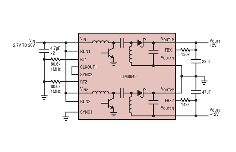
However, by using the LTM8049 μModule series, it is now possible to configure positive and negative power supplies using an extremely simple circuit configuration that includes peripheral components such as inductors and power FETs (Figure 3).
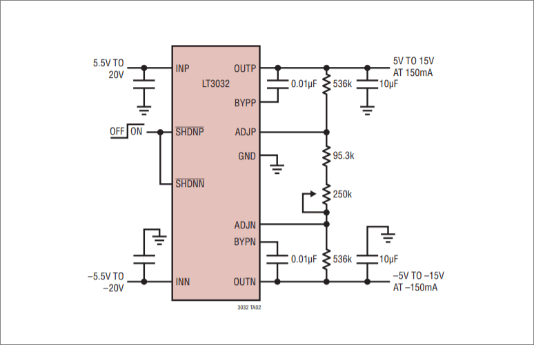
Since the LTM8049 is a switching regulator, when used in an analog circuit, a linear regulator must be inserted in the subsequent stage. For load currents of less than 150 mA maximum, the circuit configuration can be simplified by using the LT3032, a one-chip solution linear regulator (Figure 4).
The LTM8049 and LT3032 allow two ICs to form a low noise plus/minus power supply that can be used in analog circuits.
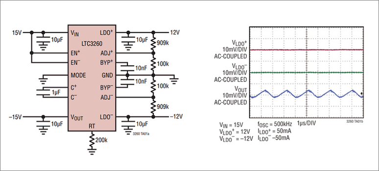
You might think it can't get any simpler than this, but since it's a simple analog circuit, if you can say "It's okay for currents up to 50mA!", a one-chip solution is possible. It is possible to use the LTC3260, which contains the configuration of a charge pump and linear regulator on a single chip.
The output passes through a linear regulator, making it possible to obtain a low-noise power supply. This is an ideal solution when there are a few analog circuits in the front-end circuit.
Click here for recommended seminars/workshops
Click here for recommended articles/materials
Click here to purchase products
Click here for manufacturer site/other related links
Inquiry
If you have any questions regarding this article, please contact us below.
Analog Devices Manufacturer Information Top
If you want to return to Analog Devices Manufacturer Information Top, please click the button below.