- Semiconductor BusinessHOME
- Products and Services of Macnica,Inc.
-
technical information

-
Events and Seminars
- Handling Manufacturer
- Support
- Inquiry
- Click here to purchase products
- Semiconductor business e-mail magazine registration
![]()
![]() Narrow down by specifying conditions
Narrow down by specifying conditions
現在2168件がヒットしています。check
The ADP5072 features independent control of positive and negative power supplies
When designing analog circuits, there are cases where not only a positive power supply but also a negative power supply is required for various sensors including CCDs, operational amplifiers, A/D converters, etc.
In this case, using an IC that can supply positive and negative power supplies on a single chip not only makes it possible to miniaturize the circuit, but also reduces costs and improves reliability by reducing the number of components, as well as reducing design man-hours.
This article explains the following three major features of the ADP5072 positive and negative power supply IC.
- Independently Adjustable/Controllable Positive and Negative Supplies
- Perfect EMI/noise countermeasures
- Small size and high efficiency even for positive and negative power supplies
1. Independent adjustment/control of positive and negative power supplies
The ADP5072 has an input voltage range of 2.85 V to 5.5 V, and outputs up to 35 V/1 A for the positive supply and −30 V/0.6 A for the negative supply. The wide output voltage range is suitable for positive and negative power supply circuits in a variety of applications.
The ADP5072's internal positive and negative power supply circuits are separate and can be configured independently.
The device also features flexible start-up sequencing, allowing manual enable, simultaneous mode, and positive or negative supply priority.
Below is the internal circuit diagram of the ADP5072.

2. Perfect EMI and noise countermeasures
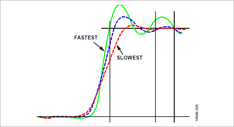
The ADP5072 contains programmable slew rate control circuitry.
This circuit reduces the slew rate of the switching node as shown in the figure below.
The result is less ringing and lower EMI.
The ADP5072 can also be synchronized with an external oscillator from 1.0 MHz to 2.6 MHz.
This feature facilitates noise filtering in noise sensitive applications.
3. Small size and high efficiency even for positive and negative power supplies
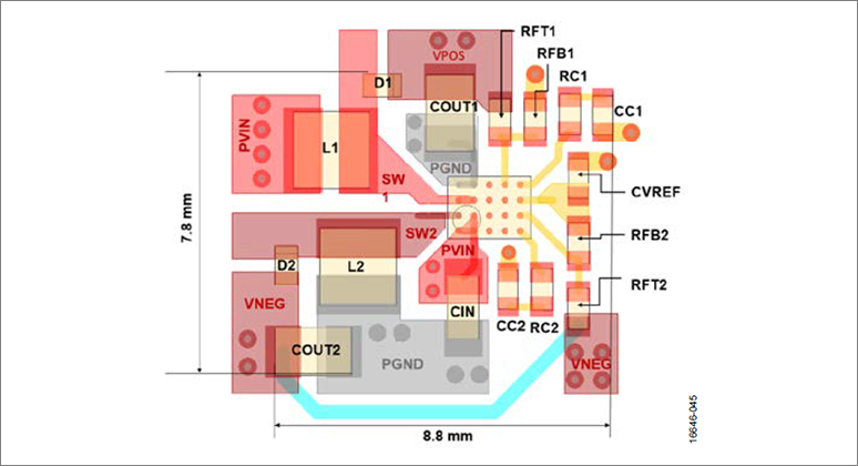
The ADP5072 is available in a small 1.61 mm x 2.18 mm WLCSP package and features a switching frequency of 1.2 MHz or 2.4 MHz, allowing the use of small inductors, making the ADP5072 suitable for space-constrained applications.
As an example, the recommended layout for an input voltage N = 3.3 V, positive supply = 12 V/100 mA, and negative supply = −3.2 V/60 mA is 7.8 mm x 8.8 mm.
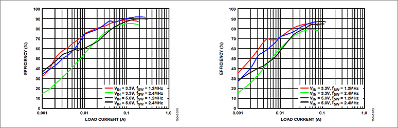
Additionally, the ADP5072's high efficiency contributes to lower power consumption in applications.
Analog Devices Positive and Negative Power Supply IC Lineup
In addition to the ADP5072, Analog Devices has released a variety of other positive and negative power supply ICs.
It is also possible to configure positive and negative power supplies by combining micro modules and LDOs.
For more information, please refer to the positive and negative power supply design.
|
Input voltage range |
2.85V to 5.5V |
2.85V to 15V |
2.4V to 16V |
|---|---|---|---|
|
output voltage |
Positive supply +35V Negative power supply -30V |
Positive supply +39V. Negative power supply -39V |
Positive supply +40V. Negative power supply -40V |
|
output current |
Positive power supply 1.0A Negative power supply 0.6A |
ADP5070: Positive power supply 1.0A Negative power supply 0.6A ADP5071: Positive power supply 2.0A Negative power supply 1.2A |
Positive supply 0.9A Negative power supply 0.9A |
|
Slew rate control |
can be |
can be |
none |
|
Sequence control |
can be |
can be |
none |
|
package size |
2.18mm x 1.61mm 20-ball WLCSP |
4mm x 4mm 20-lead LFCSP 20-lead TSSOP |
3mm x 3mm 10-Lead DFN |
Lineup of positive and negative power supply ICs
Application example
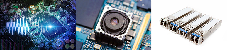
- Power supplies for operational amplifiers, A/D converters, D/A converters, etc. that require positive and negative power supplies
- CCD bias power supply
- optical module power supply
- ToF (Time of Flight) module power supply
Click here for recommended articles/materials
Click here to purchase products
Click here for manufacturer site/other related links
Inquiry
If you have any questions about this product, please contact us using the form below.
Analog Devices Manufacturer Information Top
Analog Devices Manufacturer Information If you would like to return to the top page, please click below.