- Semiconductor BusinessHOME
- Products and Services of Macnica,Inc.
-
technical information

-
Events and Seminars
- Handling Manufacturer
- Support
- Inquiry
- Click here to purchase products
- Semiconductor business e-mail magazine registration
![]()
![]() Narrow down by specifying conditions
Narrow down by specifying conditions
現在2168件がヒットしています。check

In the previous article, Let's use LTspice - Checking troublesome power supply start-up with LTspice, we introduced a method to check whether there is overshoot or a large inrush current in the output at the start-up of the regulator. Evaluation items for DC/DC converters include the following four items.
- Output ripple voltage
- Conversion efficiency
- Behavior at power supply startup (check for output overshoot and inrush current)
- Others (switch node waveform, output transient response, etc.)
This time, I will introduce how to check "4. Others (switch node waveform, output transient response)" using LTspice.
If you are just starting LTspice, we recommend that you look at the "basics" from the list below.
Let's use LTspice series list is here
Also, if you would like to see a video on how to write a basic circuit and how to execute it, there is an on-demand seminar that does not require you to enter personal information, so please take a look if you are interested. Detailed information about the seminar is also provided to those who fill in the questionnaire.
LTspice On-Demand Seminar - Function check with RC circuit -
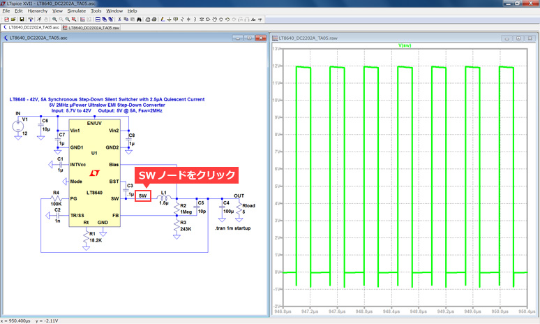
About Switch (SW) Node Waveforms
Checking the waveform of the SW pin is a very important check item to confirm that the regulator is operating normally.
We will check the circuit using the LT8640, which was used as an example in the previous article.
The specifications are input voltage Vin=12V, output voltage Vout=5V, load current Iout=1A, switching frequency fsw=2MHz.
Waveform confirmation of SW node
Then, we will perform simulation and waveform confirmation according to the following procedure.
1. You can check the waveform of the SW node by clicking the SW node (red frame) in the schematic.
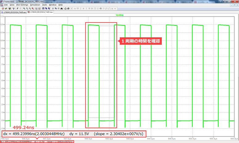
2. After confirming the waveform, next, confirm the time of one cycle.
One cycle of a switching regulator is obtained by the reciprocal of the switching frequency.
The switching frequency is set to 2MHz, so one cycle is 500ns.
When checking with LTspice, hold the mouse over the point you want to measure, and the measured value will be displayed in the lower left.
Checking the lower left value, the measured value is 499.24ns, which can be said to be normal at about 500ns.
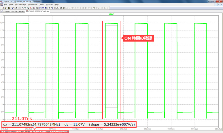
About Duty Cycle
In addition to checking whether the switching frequency (period) is as set, it is also important to check the Duty Cycle.
A switching regulator obtains the desired output by turning ON/OFF a switching element (power FET). The ratio of ON/OFF time in one cycle of this switching is called duty cycle. From the input and output voltage specifications, we can calculate the duty cycle of the buck regulator with the following formula:
Duty Cycle [%] = Vout / Vin
At the input voltage Vin=12V and the output voltage Vout=5V, which are the specifications of this time, the duty cycle is calculated to be about 41.6% (=5V / 12V).
From the LTspice simulation waveform, check if the Duty Cycle is the same as the calculation result.
Check Duty Cycle
3. Next, confirm the ON time. Check the ON time (Ton) of one cycle (T) in the same way by holding the mouse.
Checking the lower left measurement shows that the ON time is 211.07ns.
Duty cycle[%] can be obtained by (Ton / T) ×100.
(211.07ns / 499.24ns) × 100 = 42.3[%]
Since it is almost the same as 41.6% obtained from the input/output voltage ratio, it can be judged that the operation is normal.
In this way, it is possible to check the SW node waveform and calculate the Duty Cycle.
In addition to the duty cycle, there are regulations such as "minimum on time" and "minimum off time". In order to confirm these, confirmation of the waveform of the SW node is very important as an evaluation item for the power supply.
Confirmation of SW waveform when input voltage is changed
With the output voltage fixed at 5V and the input voltage under two conditions of 8V and 24V, confirm the respective SW waveforms.
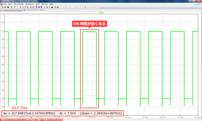
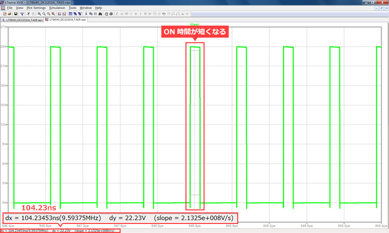
From the above results, it was found that the ON time becomes longer as the input voltage Vin decreases, and the ON time becomes shorter as the Vin increases.
You can understand this from the fact that the formula for calculating Duty Cycle is Vout / Vin.
By changing other conditions such as changing the output Vout setting, you can learn about the various behaviors of the power supply by performing simulations.
Output transient response
Output transient response refers to the response characteristics of the regulator's output voltage to sudden load changes.
In other words, it is the time and waveform to return to the set value when the voltage of the regulator drops or rises due to the load.
If the voltage fluctuation of the regulator is large, it affects the subsequent circuit (for example, FPGA core power supply etc. requires high accuracy), and if the time to return to the set value is slow, it may affect the entire system. not.
Confirmation of transient response is a very important specification in power supply evaluation.
Here, I will introduce how to check using LTspice.
Confirmation of output transient response
As with the SW node waveform confirmation, the circuit using the LT8640 will be explained here as well.
The specifications are Vin=12V, Vout=5V, fsw=2MHz.
When checking the output transient response, the load can be simulated as either a resistor or a current source.
Simulation is easier using the pulse function of the current load, so here we will introduce the method using the current source.
Then, we will perform the simulation according to the following procedure.
1. Change Rload to a current source. Select "component" from the toolbar at the top of the screen.
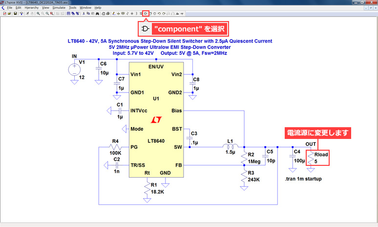
2. Select Component Symbol is displayed. Enter "load2".
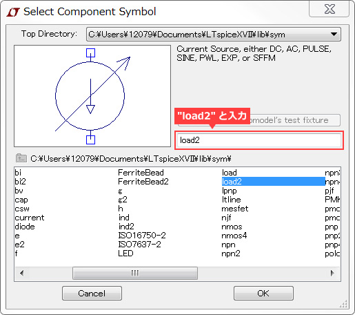
Insert it in the position where the load was with the OK button.
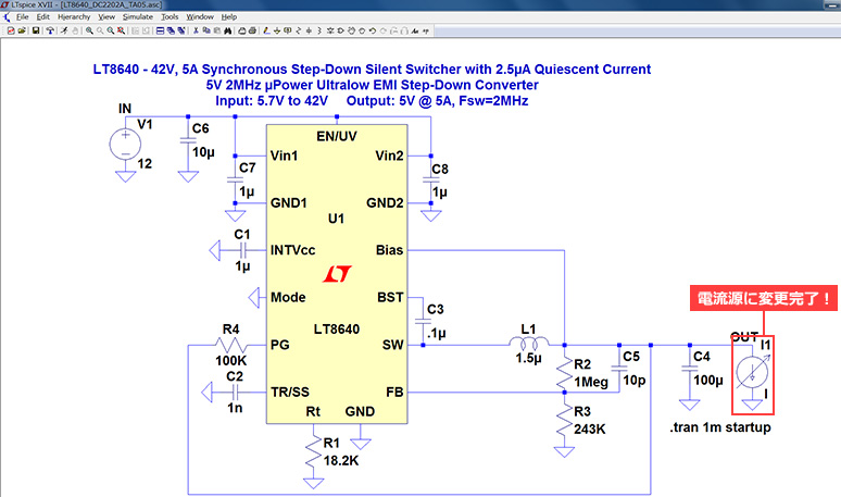
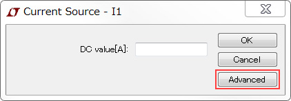
3. Right-click on the current source. Current Source - I1 is displayed, so select "Advanced".
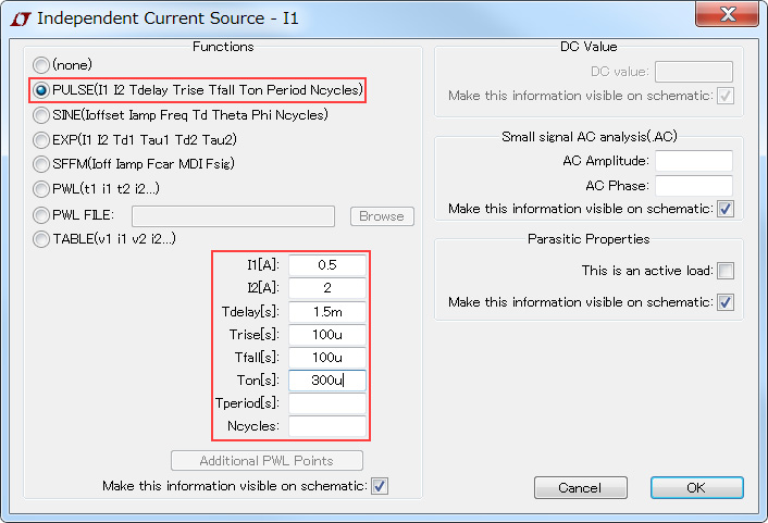
Independent Current Source - I1 is displayed. Select PULSE and enter the following values in the I1[A]-Ton[s] items.
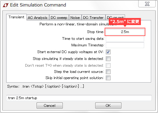
4. Finally, change the simulation run time.
Since the pulse current set above appears at 1.5ms, the simulation will end before the pulse current appears if ".tran 1m startup" is left as is.
To change it, right-click on the ".tran 1m startup" command and change Stop time to "2.5m" on Edit Simulation Command.
*Don't forget to add m (millimeters) here.
5. After completing all the above steps, press the Run button to run the simulation.
After the simulation is finished, left click on the OUT terminal and the current source.
Once you can see the two waveforms, zoom in on the transient response and click Autorange.
*For the Autorange button, please refer to the previous article.
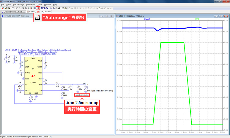
After expanding with Autorange, read the maximum and minimum values and calculate the pp value.
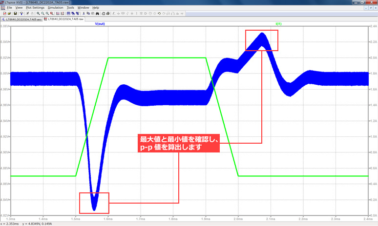
I think the accuracy requirements differ depending on the application and system. Try using mouse hold or attached cursors to see the exact values.
Output transient response characteristics generally depend on the phase compensation circuit and output capacitor. It should be noted that the results will differ depending on these constants, so it is recommended to decide the regulator circuit after careful consideration.
As introduced in this article, it can be easily confirmed by simulation, so it is important to obtain the optimum output transient response for each system while changing the circuit conditions.
At the end
Together with the previous two articles, we introduced four evaluation items for DC/DC converters.
We introduced each function using the LT8640 buck converter as an example. They can also be applied to boost and buck-boost regulators.
Toolbars (GUI buttons) and command operations can also be used in the same way for amplifiers and filter circuits.
Try applying it to the simulation of various circuits.
We also hold regular LTspice seminars for beginners. You can learn the basic operation of LTspice, so we look forward to your participation.
Click here for LTspice seminar information
Click here for recommended articles/materials
List of articles: Let's use LTspice Series
LTspice FAQ: FAQ list
List of technical articles: technical articles
Manufacturer introduction page: Analog Devices, Inc.
Click here for recommended seminars/workshops
Inquiry
If you have any questions regarding this article, please contact us below.
Analog Devices Manufacturer Information Top
Analog Devices Manufacturer Information If you would like to return to the top page, please click below.