- Semiconductor BusinessHOME
- Products and Services of Macnica,Inc.
-
technical information

-
Events and Seminars
- Handling Manufacturer
- Support
- Inquiry
- Click here to purchase products
- Semiconductor business e-mail magazine registration


 Narrow down by specifying conditions
現在2240件がヒットしています。check

As you know, FPGAs do not work unless they are configured from the flash memory that stores the FPGA's circuit data (configuration data) when the power is turned on. The flash memory must be pre-programmed with FPGA circuit data.
Being able to program the flash memory through the FPGA through the JTAG port requires only a single 10-pin header, saving BOM cost and space.
A convenient way to program through the FPGA through the JTAG port is presented. Note that Cyclone® V is used as an example, but other FPGAs can also be used.
Overview of JIC programming
When you select Active Serial (AS) mode as the configuration method for Altera® FPGAs, the device used to store the FPGA image is an FPGA serial configuration device such as an EPCQ device or an EPCS device. Programming these EPCQ and EPCS devices is done using an FPGA download cable (such as USB-Blaster™ or USB-Blaster™ II), and there are two methods for programming: direct programming and programming via the FPGA.

The direct programming method is called AS programming, and it allows you to program POF files generated by Quartus® Prime / Quartus® II development software directly. However, a separate 10-pin header (connector) must be provided on the board, in addition to the one used for the JTAG port.
Header headers for JTGA ports are frequently used for debugging, so they are almost always implemented. This means that two identical 10-pin headers are required, increasing both component cost and installation space.

If programming can be done via the FPGA from the JTAG port to the EPCQ/EPCS device, only one 10-pin header is needed. JTAG Indirect Configuration (JIC) Programming That's what it's called.
Workshop (Quartus® Prime Introductory Trial) Terasic Corporation, which is used in [the project] Cyclone® V GX Starter Development Kit This example will be used to explain how to use JIC programming.
Please note that if you are using USB-Blaster™ II or USB-Blaster™ for the first time, you will need to install the drivers for each programming hardware. If you have not yet installed the drivers, please see here.
[TIPS] Let's try installing the USB-Blaster™ II driver.
[TIPS] Try installing the USB-Blaster™ driver.
Generating and writing JIC files
environment
- Tools: Quartus® Prime v16.1
- Development Kit: Cyclone® V GX Starter Development Kit (Terasic)
procedure
- Creation of JIC file (SOF file → conversion to JIC file)
- Writing JIC files
Creation of JIC file (SOF file → conversion to JIC file)
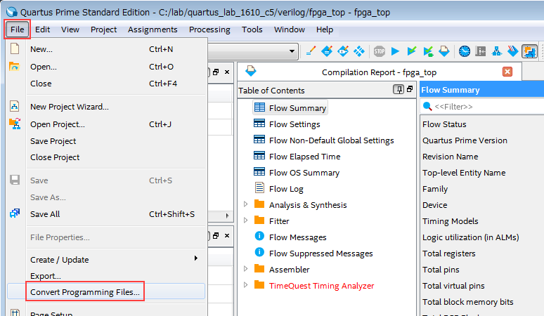
Select Quartus® Prime / Quartus® II File menu ⇒ Convert Programming Files.
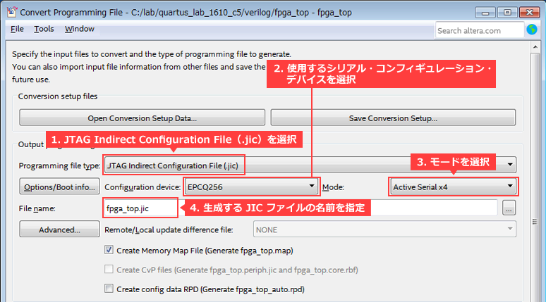
When the Convert Programming Files window opens, make the following settings.
- Select the type of programming file to generate
- Select JTAG Indirect Configuration File (.jic)
- Select configuration device
- Select EPCQ256 as implemented in the Cyclone® V GX Starter Development Kit
- Select mode
- Select Active Serial x4
- Specify the name of the JIC file to generate
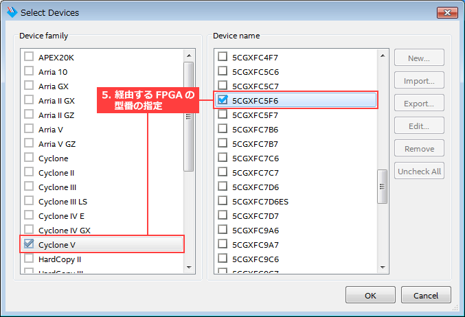
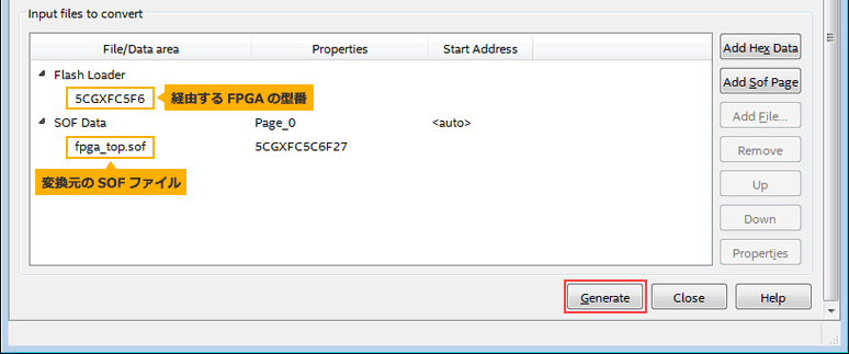
Next, specify the FPGA to be routed.
- Specify FPGA to go through
- Device family specifies Cyclone V
- Specify 5CGXFC5C6 as the device name
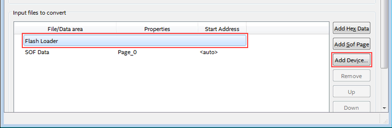
Also specify the source SOF file.
- Specify source SOF file
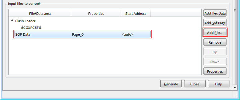
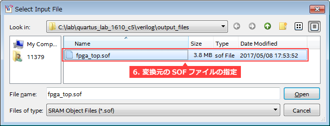
Once you have made the necessary settings, click Generate to generate the JIC file.
Was it generated successfully?
Writing JIC files
Prepare and connect the board and download cable.
Many development kits have a download cable function on the board, so you can recognize the download cable simply by connecting the PC and the development kit with a USB cable. This case also applies to this case.
For your own board, connect the download cable to the 10-pin header for JTAG.
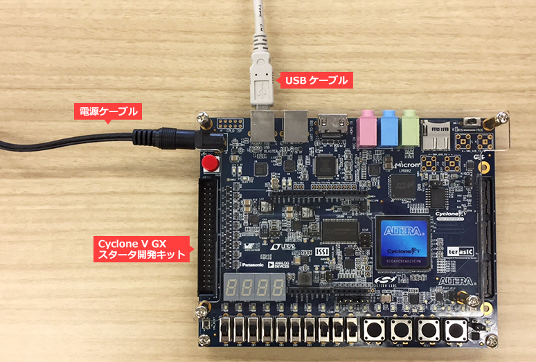
Power on the board (development kit). Then select Tools menu ⇒ Programmer in Quartus® Prime / Quartus® II or click the toolbar to start the Programmer.
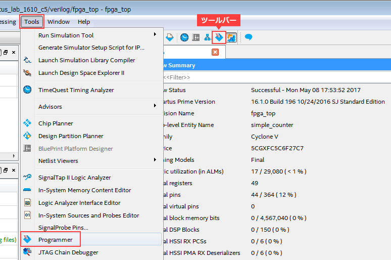
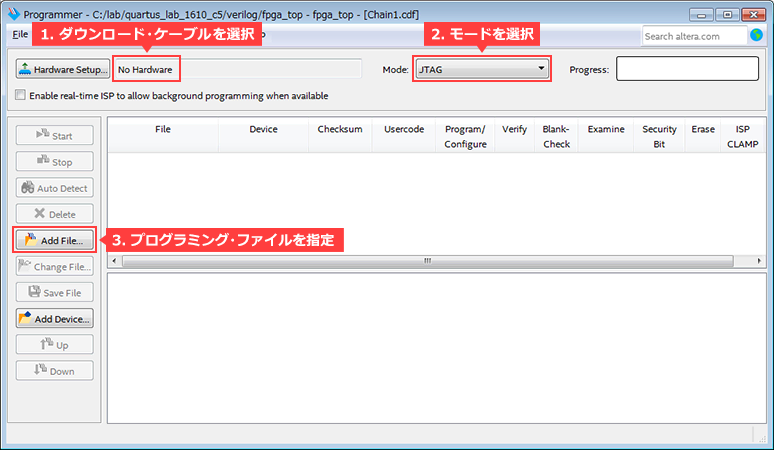
After the Programmer starts, make the following settings.
- Select Download Cable
- Select USB-Blaster
- Select mode
- Select JTAG
- Specify programming file
- Click Add File and specify the JIC file
When it looks like the image below, check Program/Configure and click Start. It will take some time to write, so please wait until it finishes.
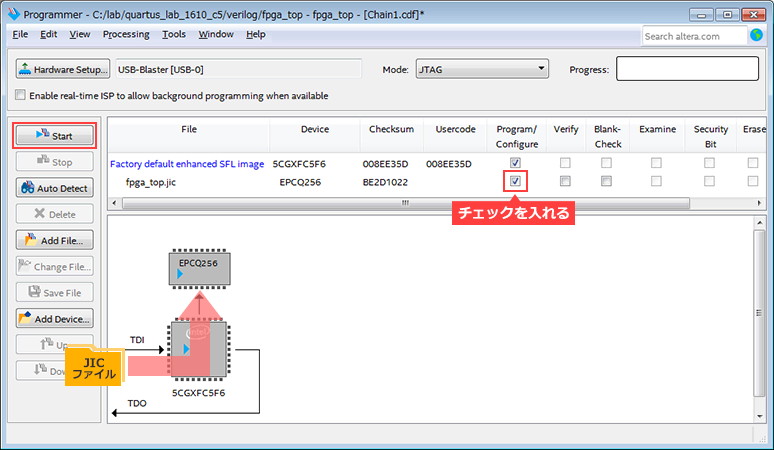
After programming is complete, turn the power off and on again. The new FPGA image is then configured and the FPGA is up and running.