- Semiconductor BusinessHOME
- Products and Services of Macnica,Inc.
-
technical information

-
Events and Seminars
- Handling Manufacturer
- Support
- Inquiry
- Click here to purchase products
- Semiconductor business e-mail magazine registration

Product Summary

Micron Technology's DDR5 SDRAM products offer up to twice the available bandwidth compared to DDR4, achieving transfer speeds of 6400MT/S.
By eliminating the memory access bottleneck that existed previously, it becomes possible to handle the large amounts of data access required for applications such as AI learning and inference, generative AI, and data analysis.
Product lineup
|
type name |
MT60B4G4RZ-56B:D |
MT60B2G8RZ-56B:D |
MT60B1G16HD-56B:D |
|
capacity |
16Gb |
||
|
data width |
x4 |
x8 |
x16 |
|
package |
78-ball (7.5mm x 11mm) |
78-ball (7.5mm x 11mm) |
102-ball (7.5mm x 14mm) |
|
speed graycode |
DDR5-5600(2800MHz), CL = 46 |
||
|
operating temperature |
0℃ to +95℃ (IT products: -40℃ to +95℃ please contact us) |
||
|
type name |
MT60B6G4RW-56B:B |
MT60B3G8RW-56B:B |
MT60B1536M16RV-56B:B |
|
capacity |
24Gb |
||
|
data width |
x4 |
x8 |
x16 |
|
package |
78-ball (8mm x 11mm) |
78-ball (8mm x 11mm) |
102-ball (8mm x 14mm) |
|
speed graycode |
DDR5-5600(2800MHz), CL = 46 |
||
|
operating temperature |
0℃ to +95℃ |
||
*For devices with speed grades and operating temperatures not listed in the table, please contact us individually.
Major new features of DDR5
Lower voltage
Lowering the VDD and VDDQ voltages contributes to lower power consumption.
DFE (decision feedback equalizer)
It can open the data eye inside the device and reduce the effects of inter-symbol interference (ISI).
DCA (Duty cycle adjuster)
This circuit can adjust the DQ/DQS duty cycle during reading, correcting the small duty cycle distortion that naturally occurs when passing through the PCB, and ultimately optimizing the duty cycle of the DQ/DQS signal received by the controller. Masu.
Click here for other new features
DQS inteval oscillator
A circuit that allows the controller to monitor delay changes in the DQS clock tree caused by voltage/temperature changes, allowing the controller designer to determine if retraining is required to optimize write timings.
new training mode
In addition to the write leveling training mode installed in DDR4, a new training mode for read preamble, command and address, and chip select has been adopted to enable high-speed data transfer.
Dedicated mode register
It holds read training patterns in a dedicated mode register. Provides tighter timing margins for high-speed data transfers.
Internal reference power supply
An internal reference power supply for command/address and chip select is installed. In addition to VREFDQ, the internal reference power supplies of VREFCA and VREFCS improve the voltage margin and enable faster data transfer.
Issues with DDR4 Expansion of bandwidth by multi-core
Next-generation processors will improve performance by increasing the number of installed cores and enabling parallel processing. Due to the increase in the bandwidth required by the system due to multi-core, there are more cases where the transfer speed of DDR4 cannot meet the specifications.
In the graph below, although the bandwidth required for one core (green line) is almost constant, the bandwidth required as a system (light blue line) increases as the number of processor cores (yellow line) increases. You can see it expanding.
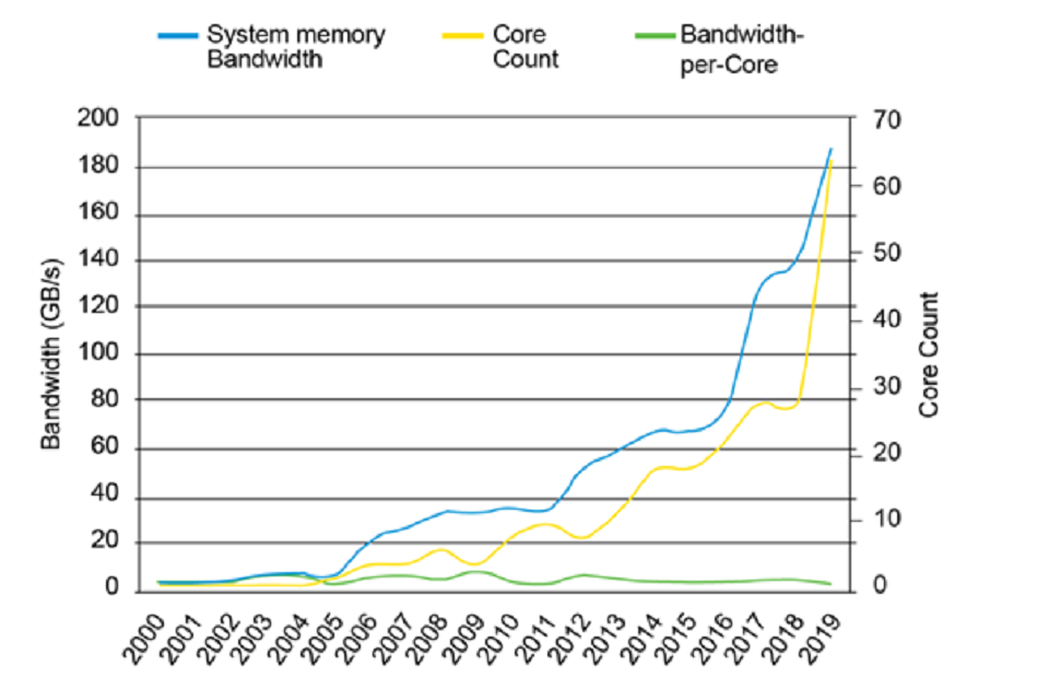
Source: https://assets.micron.com/adobe/assets/urn:aaid:aem:f1706cdb-4b55-4568-84bc-b7ee42f46236/renditions/original/as/ddr5-more-than-a-generational-update-wp.pdf
DDR5 Increases Transfer Speeds and Solves Bandwidth Challenges
DDR5 improves the transfer speed, and the standard defines it as 6400 MT/S, which is double that of DDR4.
From the transfer speed simulation results below, you can see that DDR5 has 1.36 times the bandwidth compared to DDR4 with the same transfer speed of 3200MT/s, and DDR4-3200 and DDR5-4800 have 1.87 times the bandwidth.
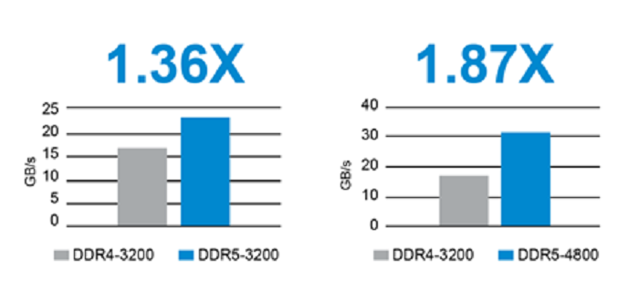
Source: https://assets.micron.com/adobe/assets/urn:aaid:aem:f1706cdb-4b55-4568-84bc-b7ee42f46236/renditions/original/as/ddr5-more-than-a-generational-update-wp.pdf
As another improvement, the power supply voltage has been reduced from 1.2V for DDR4 to 1.1V for DDR5 to improve power efficiency.
Burst Length and Bank Group are doubled compared to DDR4, and DDR5 is devised to efficiently speed up data transfer.
For other items, please check the product specifications below.
Product Specifications
|
Product series |
DDR4 SDRAM |
DDR5 SDRAM |
|
data transfer rate |
1600~3200MT/S |
3200~6400MT/S |
|
VDD/VDDQ/VPP |
1.2V/1.2V/2.5V |
1.1V/1.1V/1.8V |
|
Internal reference power supply |
VREFDQ |
VREFDQ, VREFCA, VREFCS |
|
Component capacity |
2-16Gb |
8-64Gb |
|
Prefetch |
8n |
16n |
|
Burst Length |
8 |
16 |
|
Bank groups (BG)/banks |
4 BG x 4 banks |
8 BG x 2 banks (8Gb x4/x8)4 BG x 2 banks (8Gb x16)8 BG x 4 banks (16-64Gb x4/x8)4 BG x 4 banks (16-64Gb x16) |
|
Page size |
512B/1KB/2KB |
1KB/1KB/2KB |
|
One-Die ECC |
× |
〇 |
|
DQ receiver equalization |
× |
Multi-tap DFE |
|
DCA(Duty cycle adjustment) |
× |
DQS and DQ |
|
PRECHARGE commands |
All bank and per bank |
All bank, per bank, and same bank |
|
REFRESH commands |
All bank |
All bank and same bank |
|
Training mode |
write leveling |
write leveling read preamble command and address chip select |
|
Internal DQS delay monitoring |
× |
〇 |
|
Read training patterns |
DDR4: using MPR |
DDR5: Uses dedicated Mode Register |
|
Package |
78 BGA/96 BGA |
82 BGA/102 BGA |
Source: https://assets.micron.com/adobe/assets/urn:aaid:aem:f1706cdb-4b55-4568-84bc-b7ee42f46236/renditions/original/as/ddr5-more-than-a-generational-update-wp.pdf
Contact Us


Manufacturer reference material
Introducing Micron DDR5 SDRAM: More Than a Generational Update
Related page
- Micron Technology DRAM product page
- Micron Technology DDR3 SDRAM
- Micron Technology DDR4 SDRAM
- Micron Technology LPDDR4/4X SDRAM
- Micron Technology LPDDR5/5X SDRAM
- Backward compatibility of DDR4 – How to check transfer speed and latency (CL, tAA) –
- Basics of DRAM Part 1: Read/Write Principles and Internal Structure
- DRAM Basics Part 2: Commands and Sequences
- If you are interested in memory software, please also check Tuxera products that deal with file systems