- Semiconductor BusinessHOME
- Products and Services of Macnica,Inc.
-
technical information

-
Events and Seminars
- Handling Manufacturer
- Support
- Inquiry
- Click here to purchase products
- Semiconductor business e-mail magazine registration
![]()
![]() Narrow down by specifying conditions
Narrow down by specifying conditions
現在2183件がヒットしています。check

Overview
SiC JFETs have been considered ideal devices for solid-state breaker/power controller applications because of their ability to provide low on-resistance at high voltage ratings without compromising their ability to limit current when needed.
In this article, we propose the use of normally-off SiC cascode JFETs in a dual-gate configuration to simplify the development of high-current DC and AC circuit breakers.
Other SiC Cascode JFET Applications
Much research has been done on the advantages of solid-state breakers, which can be broadly divided into hybrid breakers and complete solid-state breakers without mechanical parts.
This article will focus on solid state breakers. Table 1 outlines the advantages and disadvantages of solid state breakers compared to traditional electromechanical breakers and relays. It is known that the main advantage of solid-state breakers is their ability to interrupt current in nanoseconds/microseconds instead of milliseconds required by mechanical breakers. This becomes increasingly valuable when interrupting power sources with very low internal impedance, such as EV batteries.
It can also be used to cut off DC circuits, so no arc countermeasures are required. With no moving parts or contact deterioration, field replacement is not required and more failure modes can be prevented. However, solid-state breakers have a higher resistance than mechanical contacts, so they cost significantly more. As the voltage rating of a semiconductor increases, the same area of material used will have a higher resistance of V 2 or V 2.5 (for a basic unipolar device). This means that as the voltage class of the breaker increases, there is a direct impact on cost.
| Features | solid state breaker (Si/SJ/SiC/IGBT/IGCT) |
electromechanical breaker |
| Full controllability | ☆☆☆☆☆ | ☆☆☆ |
| High speed | ☆☆☆☆☆ | ☆☆ |
| Conduction loss | ☆☆ | ☆☆☆☆☆ |
| No arcing | ☆☆☆☆☆ | ☆☆ |
| Use cycles : no maintenance | ☆☆☆☆☆ | ☆☆ |
| Cost per amp | ☆☆ | ☆☆☆☆☆ |
| Voltage rating vs. on Rds(on) | ☆☆☆ | ☆☆☆☆☆ |
Table 1: Comparing Features of Solid State and Electromechanical Breakers
Why SiC is used in circuit protection
The primary function of a solid-state breaker is to pass on-state current with minimal resistive losses and to be able to interrupt this current on command from the system controller. At low voltages (below 600V), silicon MOSFETs have low resistance and are a cost-effective choice for building circuit breakers, relays and E-fuses, and are already being used as such in 48V battery systems.
However, above 600V, even advanced silicon technologies such as SJ (Superjunction) MOSFETs have too high a resistance. IGBTs have very low resistance, but the conduction characteristic becomes stepped, leading to excessive power losses during conduction and the resulting need for more heat removal. At voltages above 3000V, IGCTs are used to implement circuit breakers.
Figure 1 shows the evolution of specific on-resistance for silicon SJ MOSFETs, GaN FETs, SiC MOSFETs, and SiC-JFET-based SiC cascode JFETs. It can be seen that in the wide voltage class of 600 to 2000 V, SiC FETs have the lowest resistance per unit area. This allows the development of the most compact, cost-effective solid-state breakers with low conduction losses. This is extremely useful in applications where heat removal is a constraint.
All SiC devices are also able to withstand high instantaneous temperature rises (such as during a short circuit) and can handle four times the energy in the same unit area compared to silicon devices. This is because their wider bandgap means that much higher temperatures are required to thermally generate enough carriers to reduce the voltage blocking capability of the switch. 4H-SiC has three times higher thermal conductivity, which allows it to spread heat more effectively and operate at higher current densities compared to GaN and Si-based options.
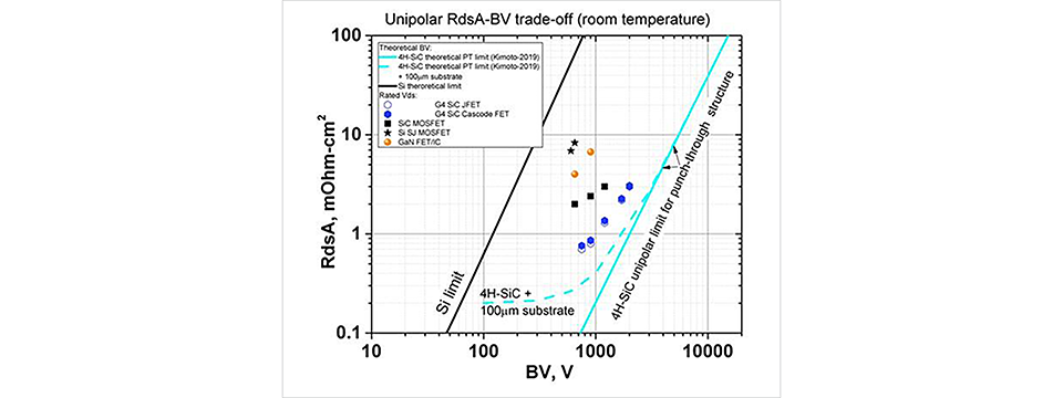
Figure 1: Comparison of specific on-resistance versus voltage for various semiconductors
Typical applications using SiC
Given that solid-state breakers generally come at a higher cost, they are likely to be used where speed, controllability, reliability, and light weight features are more important than in lower-cost applications. This is typical of any new technology, and as the technology (especially SiC) matures and scales up, costs are expected to decrease and usage will expand.
Given the rapid growth of DC sources (solar, EV batteries, energy storage, etc.) and DC loads, one area where SiC-based breakers are being considered is DC breakers, which require 750V-1200V FETs. For EV, marine, and aircraft applications where very low conduction losses are required and arc flash poses safety concerns, solid-state breakers are a good solution. The ability of solid-state breakers to rapidly interrupt a short circuit event before the current rises to >5kA or 10kA is critical. Faster coordination is possible between the main and downstream breakers in the protected circuit.
High power AC breakers also benefit from using a solid-state solution, as the on-resistance now possible with 1200V SiC FETs approaches that of mechanical breakers, and the overall solution makes maintenance in the field much easier. The increased capacity due to the fast current interruption and inrush current limiting provided by solid-state switches adds further value.
Residential AC breakers can take advantage of the unparalleled low conduction losses of SiC devices to implement smart solutions for energy management in environments with solar panels, energy storage and EVs in addition to traditional loads. Minimal heat generation allows for cost-effective breaker panels without the need for fans for cooling.
In addition to solid-state breakers, the same devices have been used to build solid-state power control devices that regulate the flow of managed power between multiple generating sources and loads on ships and aircraft. Inrush currents are managed as effectively as fault currents.
Solid-state breakers can play a role in rail networks in better managing faster fault response between the overhead lines and the system power electronics, reducing the size of the downstream power electronics, as well as their weight and cost, with benefits in system reliability and longevity.
In a variety of new applications, SiC cascode JFETs are being employed as bidirectional current limiting switches, self-powered breakers and super-cascode HV breakers.
In terms of functional safety, normally-on SiC JFETs are useful devices in applications where it is beneficial for the transistor to remain on even if gate power is lost. One can also consider a full-bridge rectifier configuration using normally-off devices on the high side and normally-on JFETs on the low side. Such a bridge would normally remain off on the input side, but the low-side JFET could short the output when both are on, thus acting as a shunt when control power is lost. Motor drive inverter designs can be improved in the same way; simply use normally-on devices as the low-side FETs and functional safety management can be simplified.
In all of the aforementioned areas, the ability for a solid-state solution to monitor its condition and allow for easily scheduled maintenance rather than post-failure repair is a major advantage, and dual-gate SiC cascode JFETs will be shown to offer the best option here.
JFET, SiC cascode JFET, and dual-gate SiC cascode JFET structures
figure 2 To SiC MOSFET and SiC cascode JFET A comparison of the basic structures is shown below. 1 Shown in SiC JFET The low on-resistance per unit area of is due to the absence of a low-mobility channel and the elimination of the need to protect the gate oxide from high electric fields with an additional shield that would add on-resistance.
but, JFET is a normally-on device, and to form a normally-off option, 2 As shown in the low voltage silicon MOSFET In a cascode configuration, SiC JFET This allows you to connect the R DS(on) To 5~15% The series-connected devices can be added to the SiC cascode. JFET A basic cascode, called LV MOS and SiC JFET It can be configured as either a dual-gate device with both gates externally accessible.
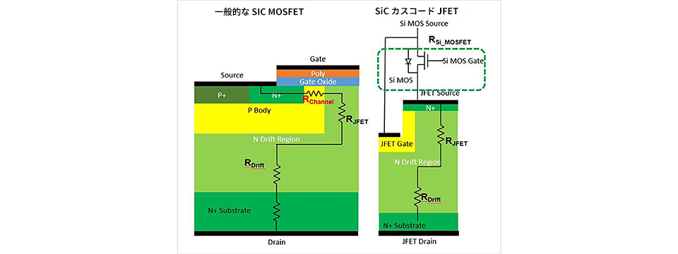
Figure 2: Difference in resistance between SiC MOSFET and SiC cascode JFET due to the lower channel resistance of the JFET
figure 3 The image on the left is the conventional MOSFET Like TO-247 Packaged in a package SiC JFET The center image shows a low voltage MOSFET The high voltage SiC JFET By stacking it on the source pad of the die, SiC FET It shows how the cascode structure is formed. SiC JFET The gate is in the package. LV MOSFET The device is normally off. MOSFET The rightmost image can be used like this: TO-247-4L In the package: MOSFET Gate and JFET Shows how both gates can be pulled out for user control.
This is a dual-gate SiC cascode. JFET(DG SiC cascode JFET) In this example, 1200V JFET The resistance of V GS =2V in 7mΩ, V GS =0V in 8mΩ SiC cascode JFET So, JFET is on 0V Close to V GS The resistor value is 9mΩ in, 1mΩ but LV MOSFET In the rightmost dual-gate device, in the on state MOSFET is turned on, JFET The gate 2~2.5V Since it can operate at , its resistance is 7mΩ The sum of the on-resistances of both is 8mΩ It will drop to. The behavior of this on-state is shown in Fig.4is shown.
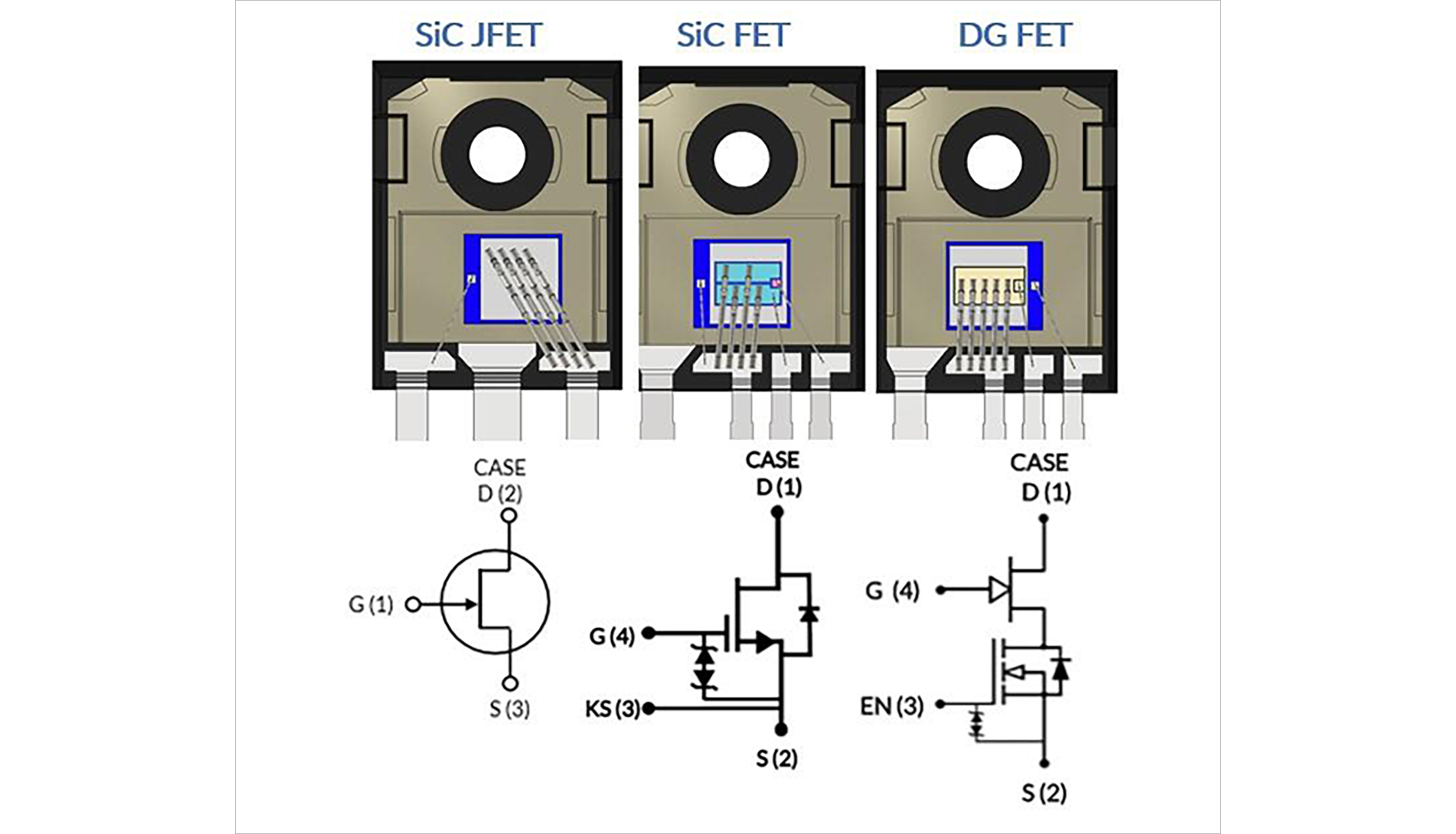
Figure 3: Structure of SiC JFET-based device
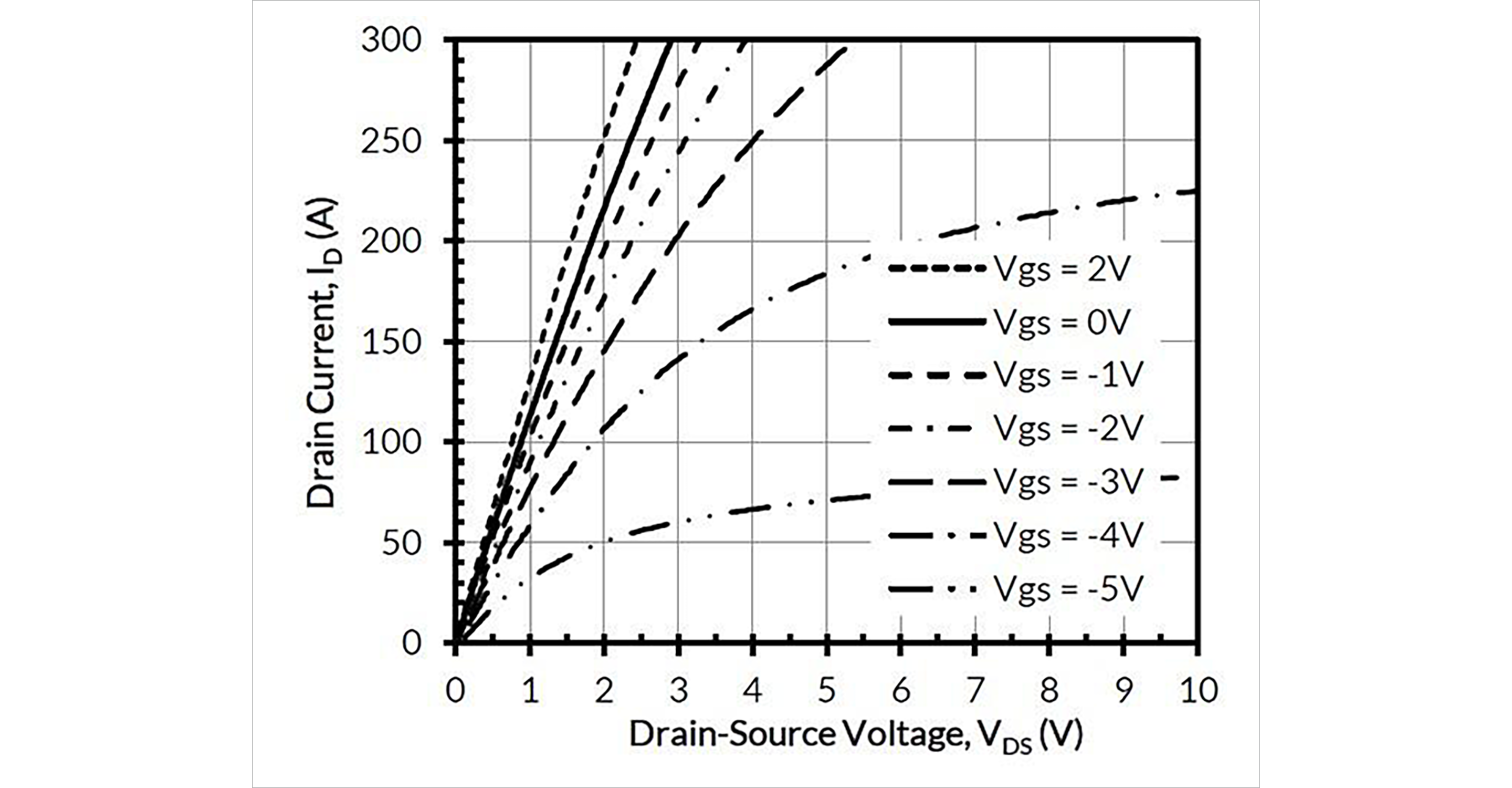
Figure 4: A lower limit of VGS=2V vs. VGS=0V is available for a 1200V dual-gate SiC cascode JFET
Figure 5 shows the JFET VGS behavior as a function of temperature at 1mA. This amounts to sensing the knee voltage of the gate-source SiCPN junction. This voltage is sensed by the gate drive circuitry when the device is on, and TJ can be determined directly. This method of finding TJ is much more accurate than finding VDS(on)=(ID∙RDS(on)).
The low-current knee voltage is immune to many process factors that change RDS(on), so it varies little from device to device. It also outperforms integrating temperature sensing diodes into SiC chips in terms of speed and accuracy. Also, temperature sensing using the power module's NTC and/or the control IC's TJ does not provide anything close to the response speed or accuracy required for this JFETVGS sensing method.
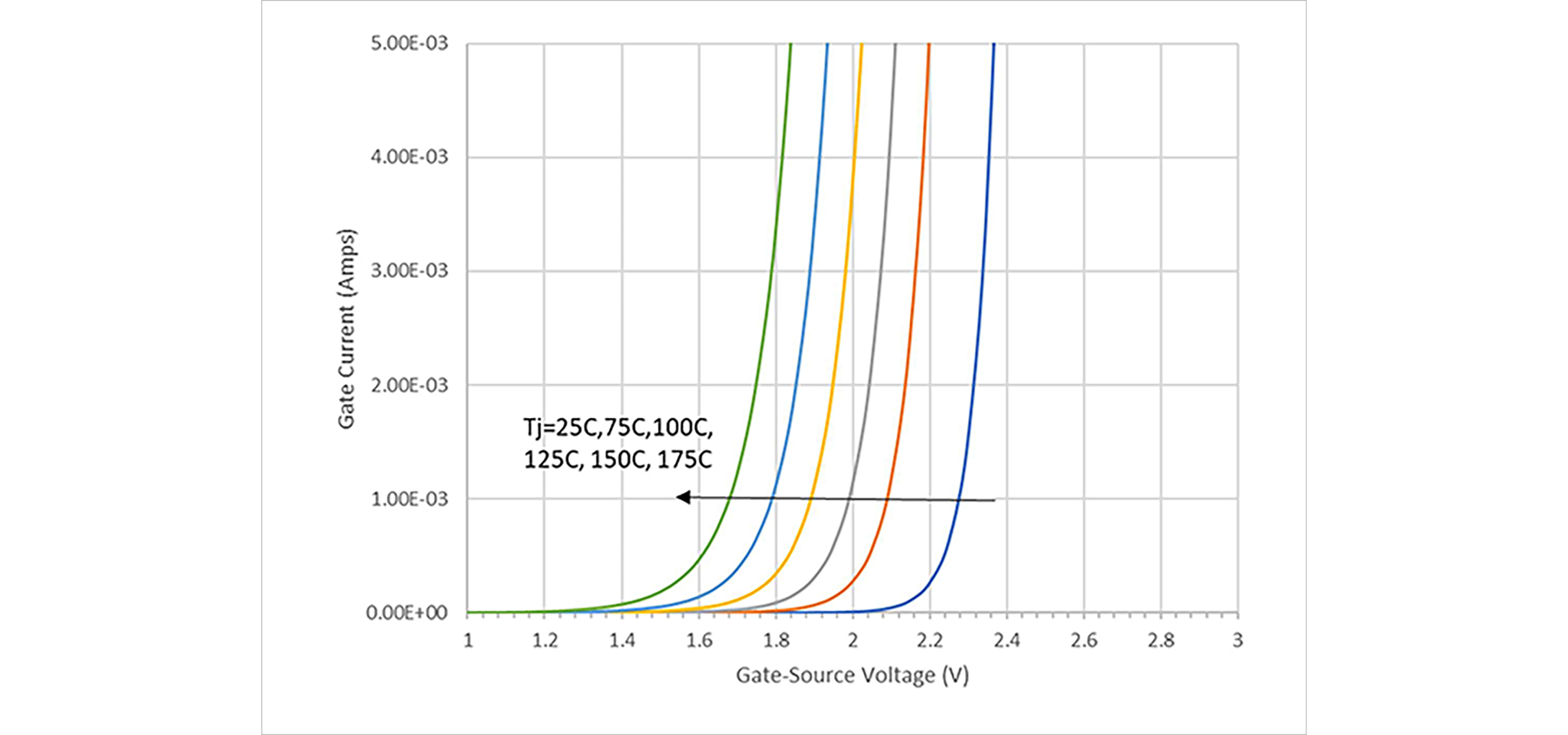
Figure 5: Junction temperature with on-VGS for SiC JFET
under known operating conditions JFET T J. Changes in can be compared to a reference to check the aging of equipment during normal operation. T. J. This indicates that if the number increases excessively, the service life may suddenly expire, enabling replacement before a fatal failure occurs. T. J. 's response speed is accurate on the microsecond scale, allowing it to monitor temperature rise within the chip during transient events such as when a breaker trips, allowing the switch to shut down before it is damaged. can also do.
simple Four terminal DG FETs at low voltage FETs The on-state drop at is measured externally V. GS and must be corrected to extract the junction temperature. For high pin count packages, of JFETs direct access to the source T. J. can improve the measurement accuracy of or, DG FETs is super low R. DS(on) logic level SMT Discrete FETs and, 2 can be implemented as one discrete, which allows JFETs Allows direct access to gates and sources.
solid state breaker
A typical circuit implementation for a solid-state breaker is shown in Figure 6. Two switches are connected at the source to provide bi-directional voltage blocking and current flow. RC snubbers (Rs, Cs) are used for individual FETs or entire FET pairs. Place a transient voltage suppression device (MOV, TVS) to absorb the induced energy from the line and the load inductance when the current is interrupted.
This architecture can be used to cover a wide range of applications. For example, in e-mobility applications, this circuit can be used to replace a switch that disconnects the DC line. All battery power is routed through solid-state switches, so a 500-1500A rated, 1200V breaker should have a resistance of a few milliohmsor less. This requires the use of many devices in parallel, and using ultra-low R DS(on) devices simplifies the circuit.
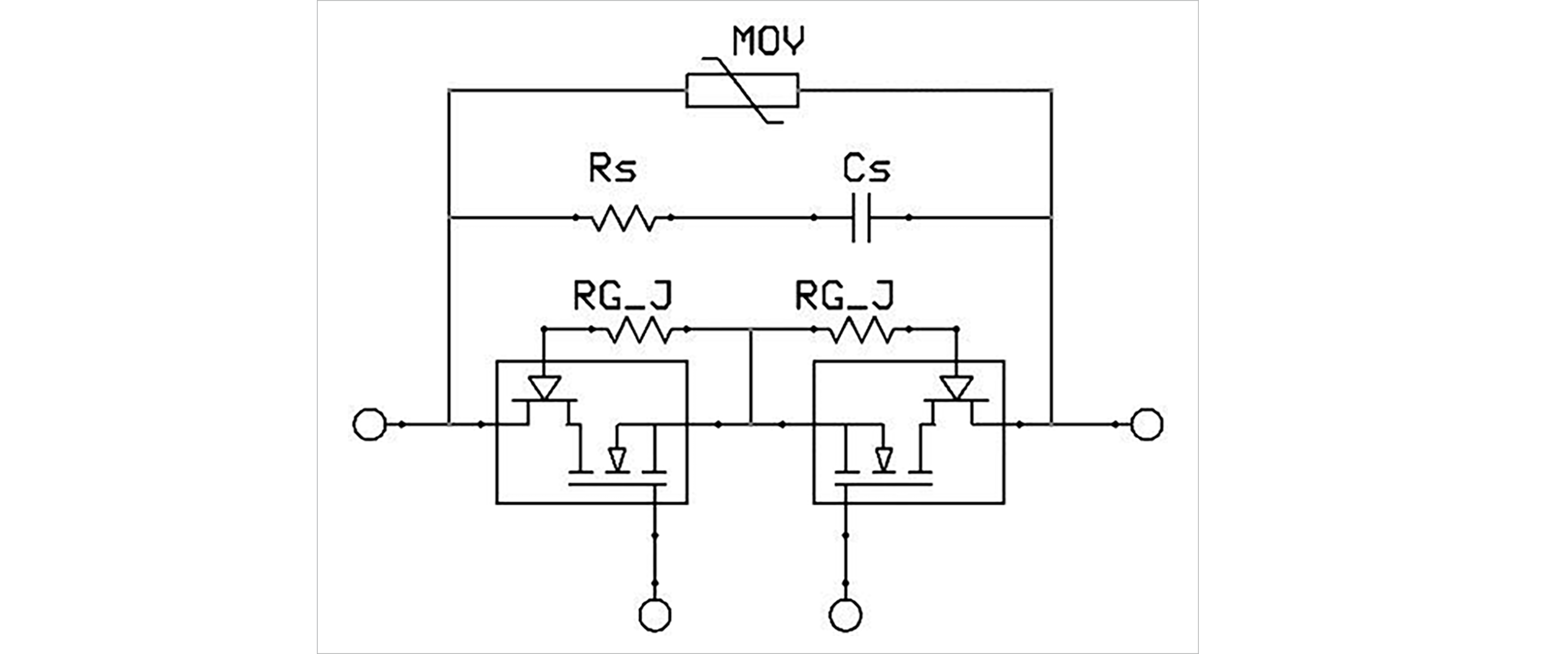
Figure 6: Circuit architecture of a solid-state circuit breaker (power element)
Figure 7 shows the experimental setup used to parallel dual-gate SiC cascode JFETs and demonstrate their ability to interrupt large fault currents. Three TO247-4L devices, 9mΩ each, 1200V, are paralleled, with each switch having a resistance of 3mΩ.
SiC Schottky diodes D1~D4 (UJ3D065200K3S) are used as TVS (instead of MOV) to protect the switch during turn-off transients.
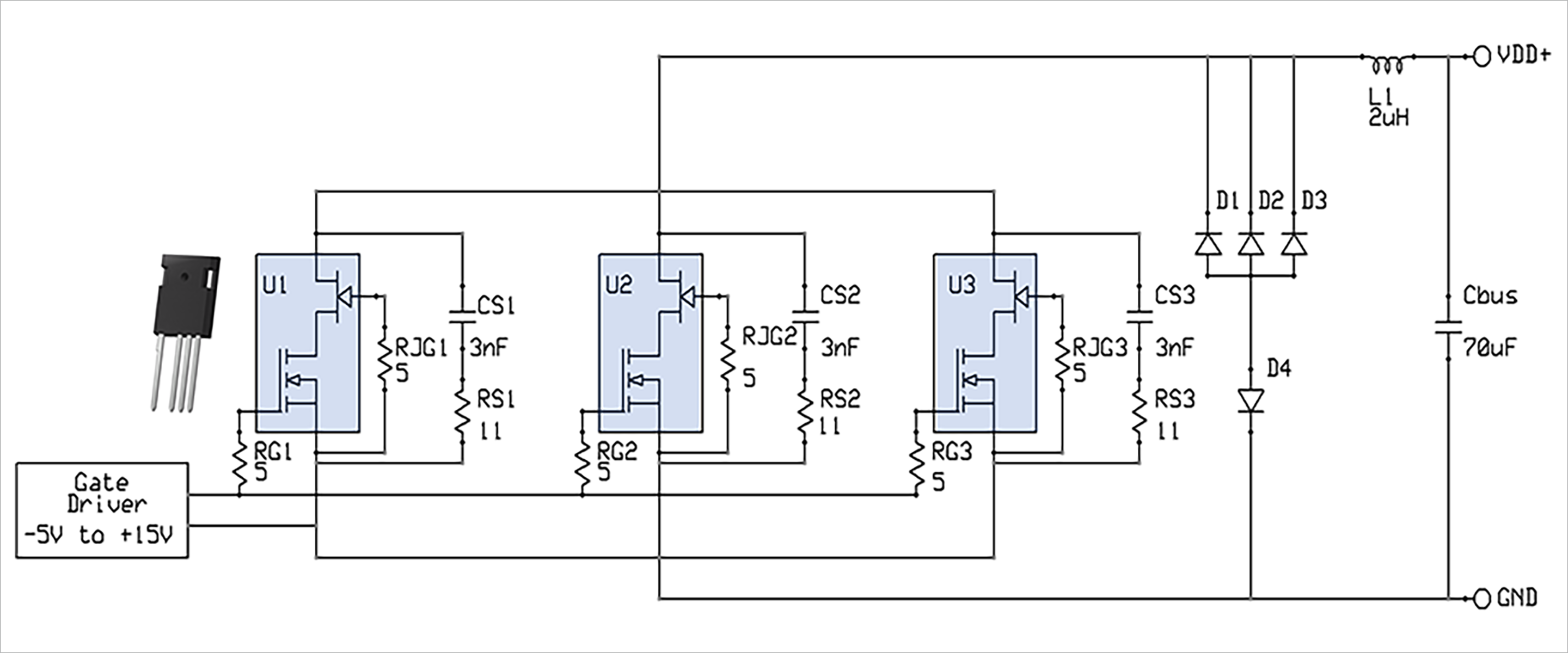
Figure 7: Schematic diagram of a solid-state circuit breaker test circuit with three dual-gate SiC cascode JFETs connected in parallel to form a switch.
The positive temperature coefficient of the device on-resistance shown in Figure 8 ensures good current sharing when the device is on. For this test, the device can be operated with a standard MOSFET like gate drive-5~15V or a 0~12V unipolar gate drive can also be used. A 5 Ω resistor is provided for each of the MOSFET and JFET gates to aid in parallel operation during switching. A 5ΩJFET R G slows the turn-off of the switch. This resistance is much larger than the internal gate resistance of the JFET and helps set the cascode turn-off speed and match the switching behavior for the three parallel devices.
Individual RC snubbers are placed across each device to minimize the stray inductance that would exist between the snubbers and the switches. The gradual variation of JFET V th with temperature (Figure 9) is also important to ensure good current share during switching transients.
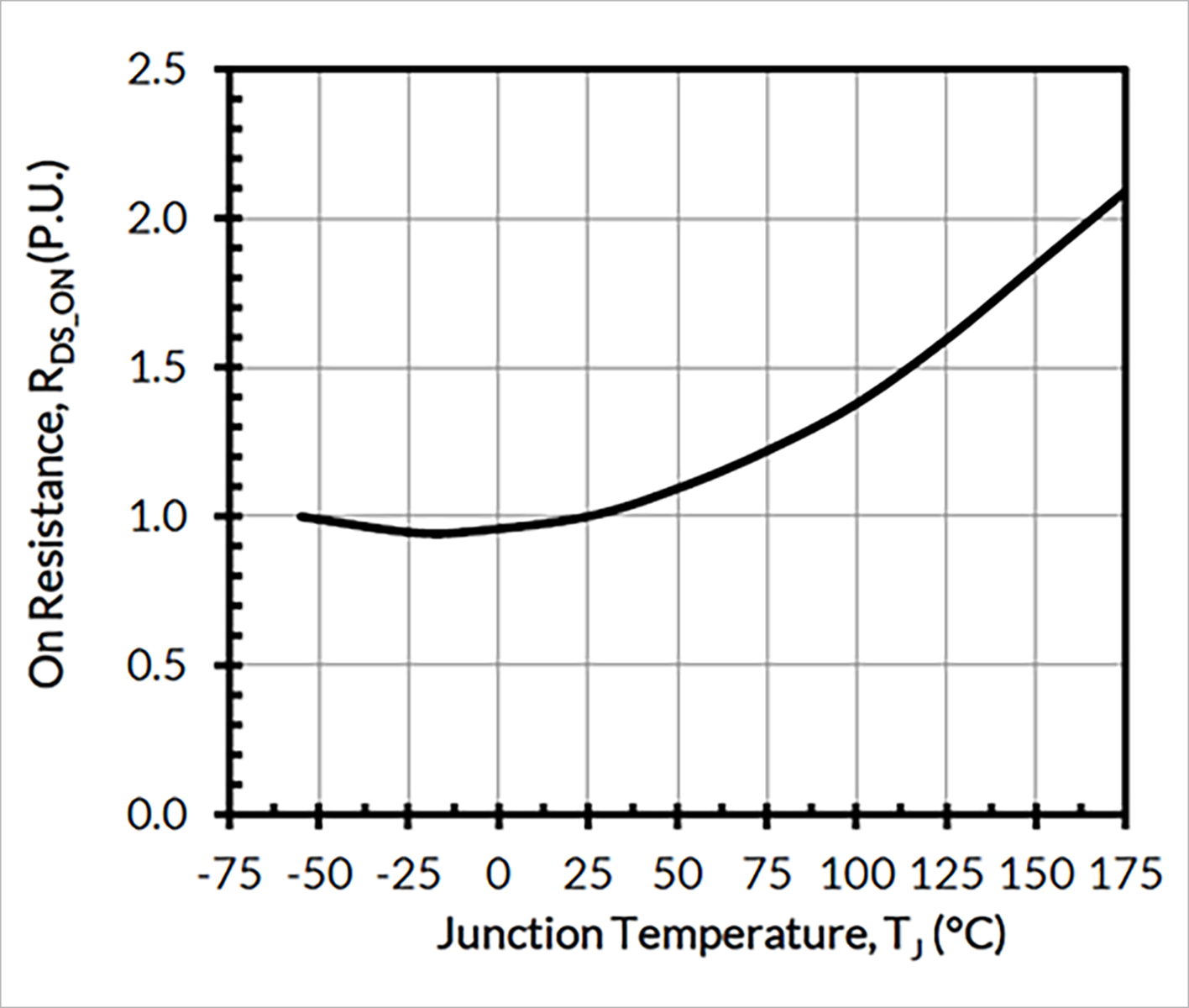
Figure 8: Temperature dependence of RDS(on) for 1200V dual gate device
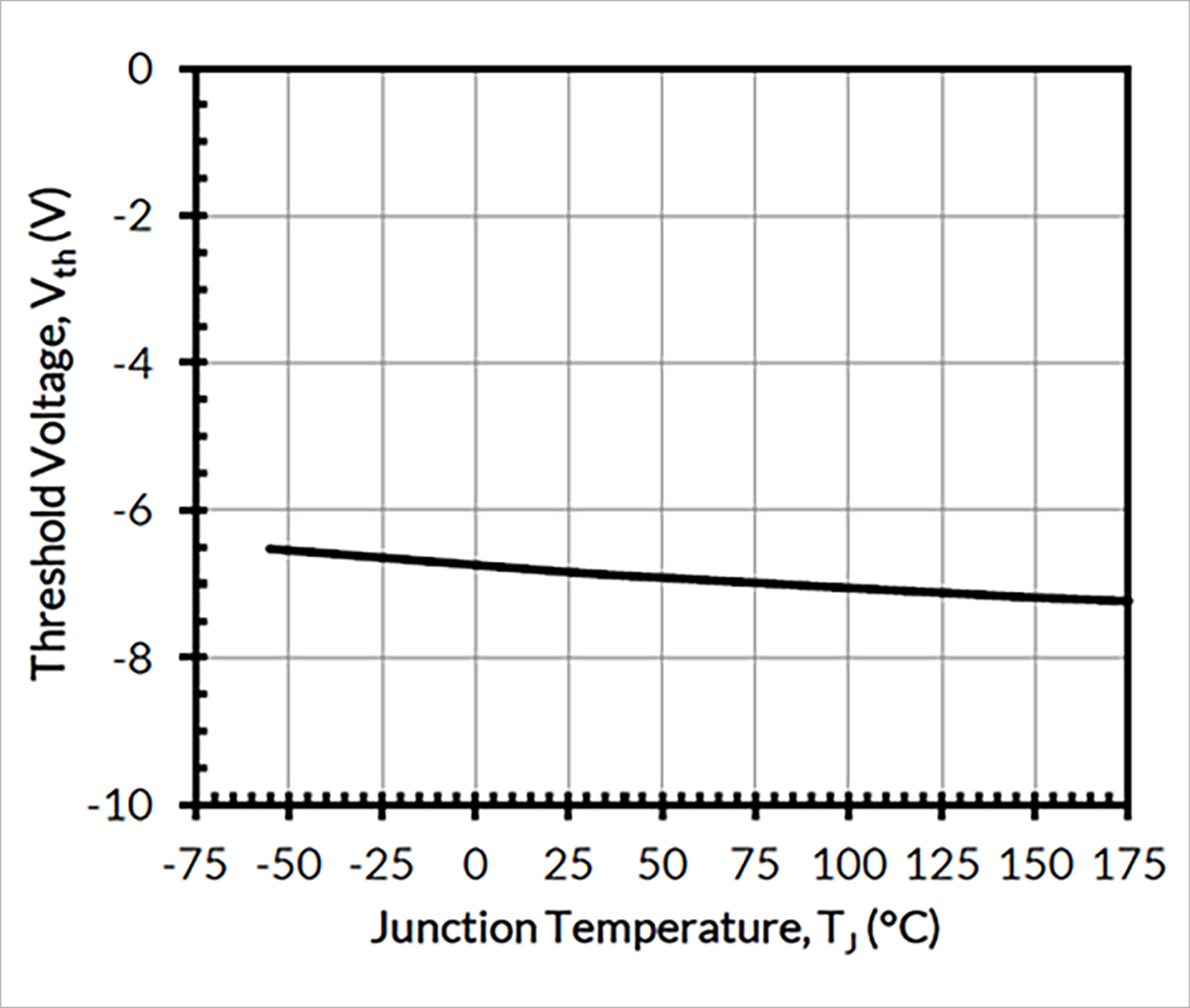
Figure 9: Temperature dependence of Vth for 1200V dual gate device
Figure 10 shows the measured turn-off behavior with three parallel-connected FETs. The bus voltage is 400V and the TVS clamp is made using a 200A, 650V SiC Schottky diode UJ3D065200K3S, capable of absorbing the avalanche energy of the 2 μH inductance used to simulate the line inductance. At 1000A, this energy is 1J, so 3 such diodes in parallel are used to give adequate margin.
A gate pulse V GS is used to ramp the current to 1150A in 10 μs and then turn off. The current in the 2 μH inductor is sustained, causing the device voltage to fly up at a rate determined by the switching speed (set by the JFET 's R G in this case) and the snubber used. When the clamp voltage set by the TVS diode breakdown is reached, the current is transferred to the TVS diode.
This arrangement allows three TO-247 devices to smoothly turn off the 1150A as shown in Figure 10. Note that the SiC FET current is interrupted in <500ns and transferred to the abalancing TVS array. The peak current sets the 5 μs duration for the current to return to 0, and the down slope is set by BV (TVS) /L1. The short voltage spikes in the V DS waveform are the result of relatively fast di/dt at switch turn-off and stray inductance between the device and the TVS diode. This can be further reduced by slowing the turn-off speed and / or adjusting the RC snubber.
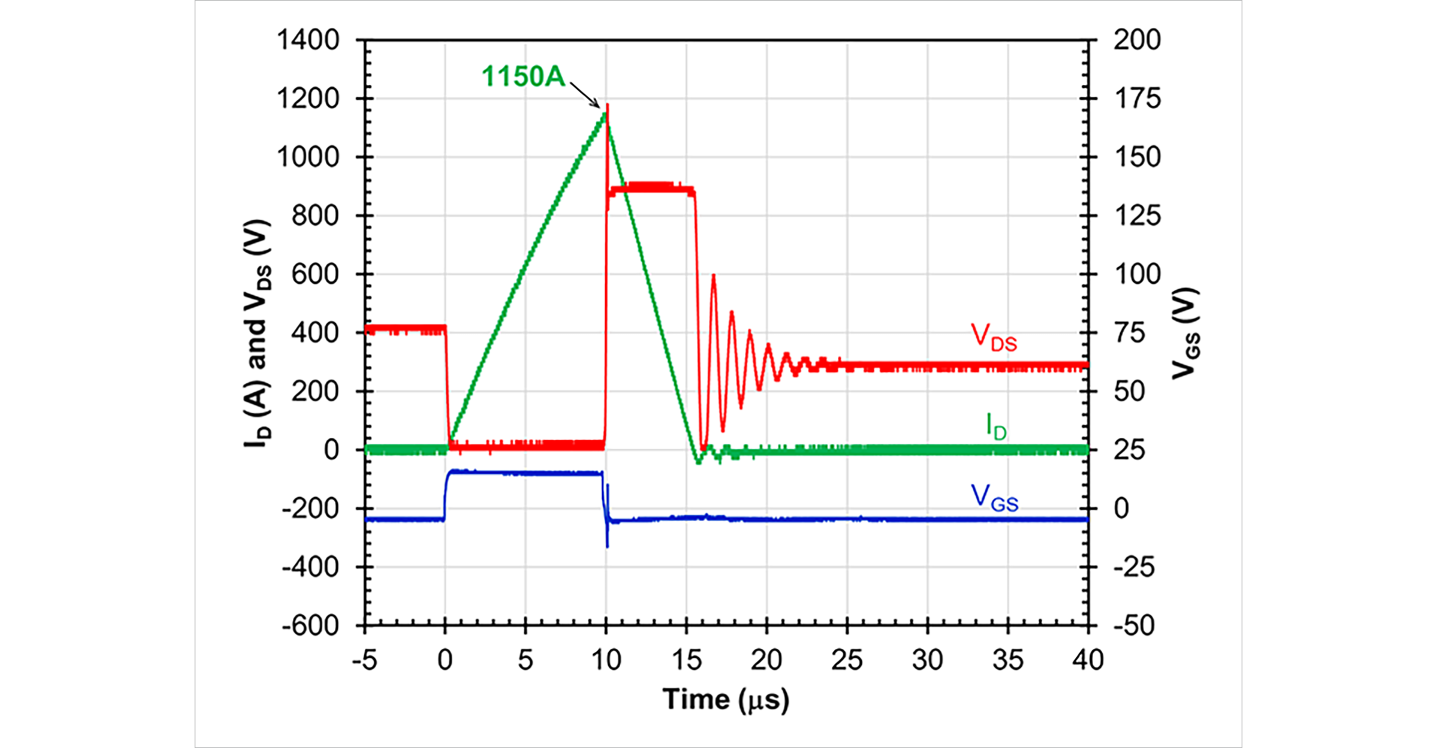
Figure 10: Measured turn-off transient waveform at 1150A for three 1200V dual-gate devices connected in parallel in the test circuit, as shown in Figure 7. TVS clamp voltage is about 900V
Figure 11 implements a dual-gate device compatibility study on a 2mΩ, 1200V module within a SOT-227 footprint, in which six such devices are used in parallel. A single 22 Ω resistor was used to slow the cascode switching, and the device was equipped with an 11 Ω, 20 nF snubber. To facilitate higher current testing, the line inductor is reduced to 0.4 μH and five 200A, 650V diodes in parallel are used as TVS.
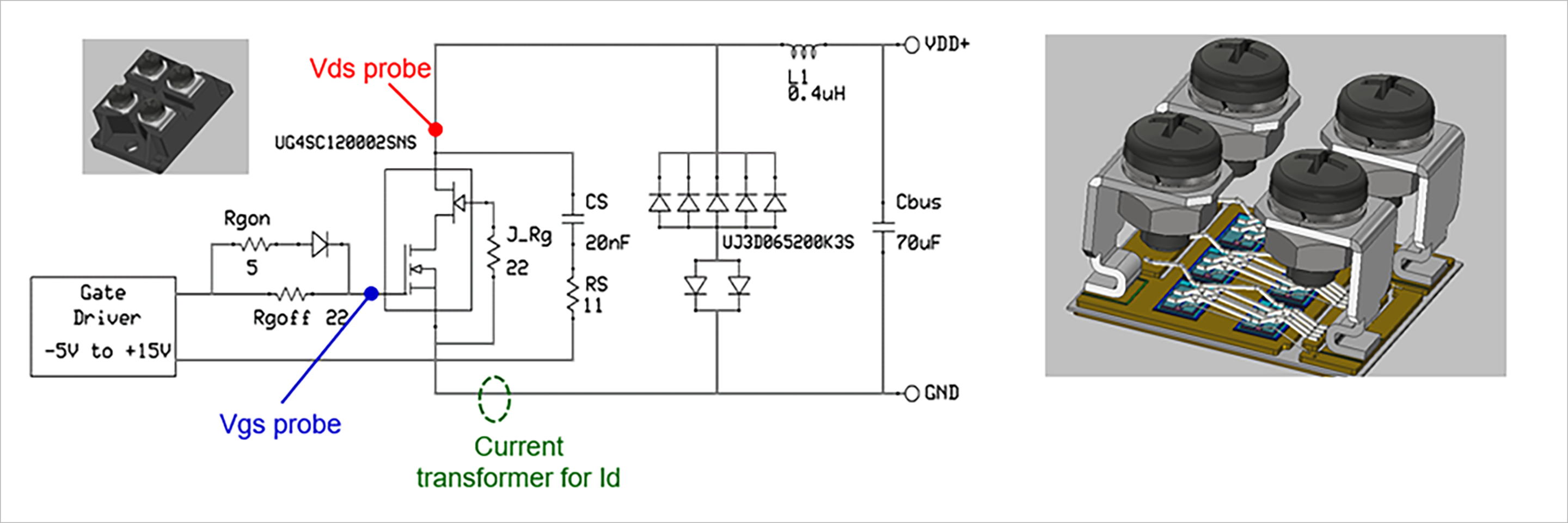
Figure 11: Schematic of a solid-state circuit breaker test circuit in which a switch is formed using a dual-gate module with a SOT-227 footprint with six 9mΩ, 1200V devices connected in parallel.
Figure 12 using the module 1950A shows the waveforms obtained from the test when interrupting the peak current of twenty two in Ω resistance JFETs Adjust turn-off, louder RC By using a snubber, V. DS Removed voltage spikes in the waveform. Including package parasitics, it provides a 2.2mΩ, 1200V device rated at over 300A.

Figure 12: Measured turn-off transient waveform at 1950 A for the 1200 V dual-gate module of the test circuit shown in Figure 11. TVS clamp voltage is about 900 V
from a commercial point of view
To fully implement a solid state breaker, use two such switches. The switch connection is common source configuration. To support even higher currents, modules with more parallel devices are being developed. These examples show the use of dual-gate devices in cascode, driven by standard silicon MOSFET/IGBT gate drivers, but a more advanced control would be to enable a low-voltage MOSFET and use a SiC JFET A possible method is to directly drive the gate of . It uses a low-voltage MOSFET as an enable switch to directly drive the gate of a SiC JFET. This allows the SIC JFET to minimize conduction losses and provide junction temperature sensing. Stacking current-sensing LV MOSFETs eliminates the need for expensive external current-sensing means.
SiC transistors can handle four times more avalanche energy than silicon. However, as the line inductance and current increases, it becomes impossible for SiC to absorb all of the avalanche stress. Therefore, parallel-connected MOV devices are used, and parallel-connected MOV devices are used. The cost of a solid-state breaker solution therefore depends on the cost of the SiC switches and MOVs used. MOVs are much more resistive in their clamping characteristics, so peak voltages are much higher than SiC TVS diodes.
Compared to the SiC TVS diode used in this demo, the peak voltage is much higher. MOV is to keep the peak voltage below the rated breakdown voltage of the SiC TVS diode. Also, as the rated voltage of the SiC element drops, the MOV to keep the peak voltage below the rated breakdown voltage of the SiC element inevitably increases. In the example given in this article, the bus voltage is in the range of 400 to 600V, so using a MOV that keeps the peak voltage below 1200V for the worst case turn-off current would result in a 1200V SiC device can be used.
In theory, a low-cost MOV capable of peak voltages of 1500-1700V would require the use of 1700V devices, which could increase the cost of SiC solutions. In this case, the SiC solution costs nearly double. So there is a direct trade-off between the cost of SiC and the cost and size of MOVs. There is a direct trade-off between MOV cost and size, scaling up with the worst-case energy the breaker must absorb. Ultimately volume and weight considerations limit breaker size in some applications, requiring higher voltage rated and more expensive SiC breakers.
The cost of SiC devices is declining rapidly with increasing adoption, and market forecasts are primarily focused on the growth potential of the EV segment for SiC devices. Volume-driven efficiencies are expected to halve the cost of SiC wafers over the next few years. Technology enhancements projected for SiC JFET technology will steadily reduce RDSA and, together with volume efficiencies, will push costs to new low levels.
Summary
Solid-state breakers using semiconductors in the 600-1200V class may be approaching a tipping point in their popularity. SiC devices are particularly well suited for this voltage class due to the lower RDSA they can offer, and SiC JFET-based solutions have been shown to excel in this regard. The overall growth of the SiC market in EVs and other applications is creating a virtuous cycle of cost savings.
Technological developments are rapidly reducing the RDSA of SiC FETs, and this trend is expected to continue over the next few years, with another 2-3x reduction in RDSA. These trends will intensify further, driving cost-effectiveness and, consequently, the adoption of solid-state circuit breakers. Understanding and leveraging all the system-level benefits of solid-state breakers and the ability of these devices to provide instrumentation to help monitor degradation, combined with trends emerging in Industry 4.0, is driving solid-state It shows that a big change occurs in the circuit. Protection can come soon.
Inquiry
If you have any questions regarding this article, please contact us below.
On Semiconductor Manufacturer Information Top Page
If you want to go back to ONSEMI maker information top page, please click below.