
![]()
![]() Narrow down by specifying conditions
Narrow down by specifying conditions
現在1887件がヒットしています。check

Ultra-high voltage SiC and Supercascodes
New applications are emerging that require high voltage switch technology with significantly lower system solution costs and operating losses than silicon IGBT and IGCT technologies. This ranges from solid state transformers, MW motor drives to smart grid applications (FACTS, STATCOM) and HV DC breakers. SiC MOSFETs are seen as an excellent breakthrough option in the near future, and Qorvo offers a unique approach to accelerate market adoption of wide bandgap (WBG) high voltage switches. doing. This approach is called Supercascode. We compare this approach and its proven performance using silicon and silicon carbide MOSFET technologies.
SiC devices and modules
There have been many advances in high-voltage SiC devices in the last decade. In theory, SiC devices can be developed to reach at least ten times the maximum voltage rating of silicon devices. Along these lines, there have been many demonstrations of single SiC MOSFETs up to 15KV and even SiC IGBTs up to 27KV. MOSFETs in the 6.5KV-10KV range are emerging as module-based products. It is well demonstrated that SiC MOSFETs offer dramatic loss reduction compared to silicon IGBTs above 3.3KV.
For 10-25KV voltage SiC IGBTs, the challenges of carrier lifetime enhancement and control, ultra-thick epitaxial layer growth, device reliability and optimal performance are being researched, and commercialization is still 5-10 years away. increase.
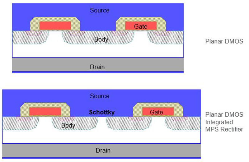
The main device structures currently in use or being developed in the >3.3KV field are planar MOSFETs and MOSFETs with integrated PiN Schottky (MPS) diodes shown in Figure 1. The latter device does not require additional SiC Schottky diodes inside the module, allowing more space for mounting MOSFETs, and less chip size increase for adding Schottky regions inside each cell. , can increase the rated current available. However, the applications we are targeting require high current ratings, requiring relatively large devices with active areas of 0.5 to 1 cm2, making it difficult to achieve high production yields in SiC.
Many such devices must be paralleled within a module to achieve the desired current rating, with each chip switching at the bus voltage.
One of the key challenges for high-voltage devices is that the thicker the epitaxial layer, the more defects the initial epitaxial wafer will have. These thick and lightly doped layers have a lot of doping variations as it becomes difficult to maintain tight doping control once the doping level reaches the 10 14 cm 3 level. Also, as the thickness increases, so does the cost of consumables used during the epitaxy process. The current state-of-the-art has achieved high quality 30um epitaxial layers up to 3.3KV devices, and enhancements are underway for 6.5kV-10kV (50-90um) layers to reach production quality in the next few years. increase. Epitaxial layers rated up to 1.7 KV are currently on the market with very high quality and tight parameter distributions on 6-inch 4H-SiC substrates.
Many interesting challenges arise when packaging ultra-high voltage switches. If one switch operates with a 5KV bus voltage and switches off in 25ns, the dV/dt will be 200V/ns. A stray capacitance of 10pF (eg, from chip drain to baseplate or across an isolation barrier in a gate circuit) produces a displacement current of 2A (C * dV/dt) per chip. Since high power modules tend to put many (10-20) chips in parallel, this problem can be very serious. These drift currents can cause additional losses and even cause serious malfunction problems in low voltage gate drive electronics. Excessive displacement current flow can also weaken the insulation of wiring and circuits within the module and externally.
On a 10KV rated device, the 10KV will drop across a 1mm zone on top of the device termination. To avoid air pockets, partial discharges, and destructive potentials in the vicinity of this field from busbars and bond wires, great attention should be paid to device encapsulation and cleanliness during module fabrication. A thick ceramic is also required to isolate the switch from the baseplate, which increases thermal resistance. For example, using a single ceramic DBC for a 15KV device requires an AIN thickness of 1mm or greater. The field distribution of the traces on the ceramic must be properly managed to control chip-to-baseplate partial discharges and ultimately catastrophic shorts within the module.
What is Supercascode? Why is this necessary?
Qorvo has developed a high voltage SiC device operating from a single gate driver using the Supercascode concept of connecting multiple low voltage devices in series. Let's examine the basic logic behind this approach. Table 1 shows the resistance values and breakdown voltage ratings for 1cm 2 SiC JFETs. Consider the example of using 6500V devices in parallel to build a 6500V, 12.5mΩ module. It requires 4 chips with an area of 1 cm 2 connected in parallel. Alternatively, the same resistance value can be achieved by placing four 1cm 2 3mΩ, 1700V chips in series (3x4 = 12mΩ). That is, the series solution uses essentially the same amount of SiC, but the lower voltage devices are clearly less costly, with higher yields, better parameter distributions, and easier manufacturing. can.
|
BV Rating |
JFET RdsA |
|
Volts |
mΩ-cm2 |
|
1700 |
3 |
|
3300 |
12 |
|
6500 |
50 |
|
10000 |
120 |
Table 1: SiC JFET on-resistance comparison from 1700V to 30KV
Note that four series-connected 1cm² chips have the same resistance as four 6.5kV parallel-connected chips. This is the basic logic of Supercascode's approach.
The same concept can be used with SiC MOSFETs, but each low voltage module would require its own synchronous gate drive. This adds more complexity. In the Supercascode scheme, one low voltage MOSFET at the bottom of the series chain controls the entire series switch. This makes the gate charge requirements of the Supercascode scheme much lower than driving parallel-connected HV MOSFETs or series-connected HV MOSFET modules. Table 2 compares the properties of the Supercascode module with those of an equivalent module with SiC MOSFETs connected in parallel.
|
Module Approach |
Conventional |
Supercascode |
|
|
SIC Chip Technology |
Die |
6.5kV MOSFET Chip |
1.7kV JFET Chip |
|
RDSA |
63 mΩ-cm2 |
3m0-cm2 |
|
|
Die size |
8.33 x 8.33mm2 |
7.7 x 7.7mm2 |
|
|
Die Max. Ron @ RT |
160 mO |
5.5mf2 |
|
|
Half-Bridge Module Technology |
Max. Ron @ RT |
20 mO |
20ma |
|
Switch Configuration |
8 dies in parallel |
5 JFETs (each has 2 dies) in parallel) in series |
|
|
Total Die Count |
16 |
20 |
|
|
Total SiC Area |
1.110 mm' |
1.186 mm-' |
|
|
Module Features |
Typical Vth @ 150*C |
2.0V |
3.7V |
|
Practical Gate Drive |
-5V to +20V |
Standard 0V to +12v |
|
|
Total Gate Charge Og |
2360nC |
100nC |
|
|
Anti-Parallel Diode |
Built-in |
Built-in |
|
|
High Orr |
Low Oc |
||
|
Knee voltage: >2V |
Knee voltage: 0.7V |
||
Table 2: Comparison of Supercascode module and SiC MOSFET with integrated Schottky diode in parallel. Notice the difference in gate charge
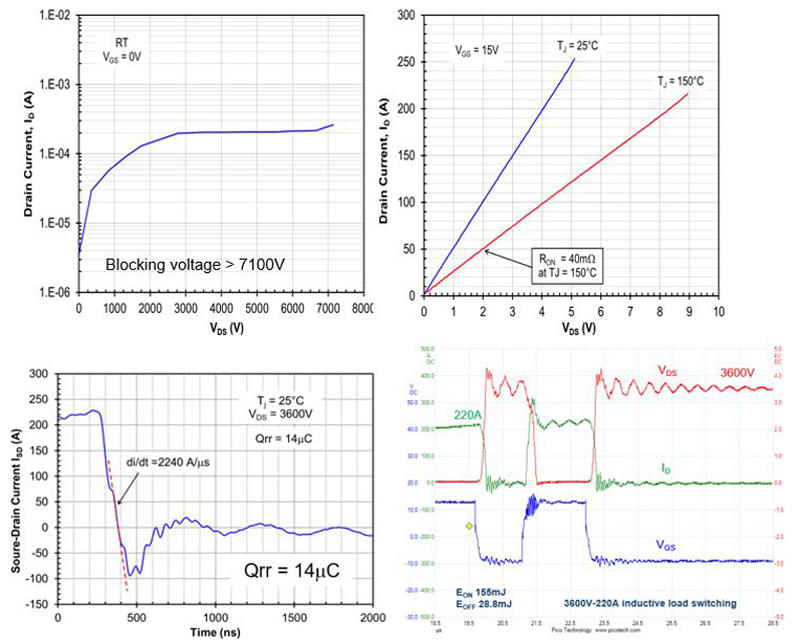
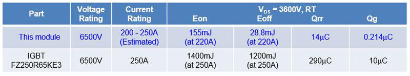
Many implementation circuits have been devised for Supercascode, but Figure 2 shows two circuits developed by Qorvo. This module requires a passive balanced network embedded within the module, as shown in Figure 3. Since losses are dominated by SiCJFETs, they are placed on a DBC (Direct Bonded Copper) substrate for efficient heat removal. Other network components are on the PCB layer above this layer. Figure 4 shows the electrical characteristics of the Supercascode module being developed at UnitedSiC. This device blocks the required voltage, with an on-resistance of 20mΩ (25°C) and a knee voltage in the third quadrant of only 0.7V from the Si MOSFET, followed by the 19mΩ resistance of the JFET in series, making it a SiC JBS diode. is not required. The diode recovery charge, QRR, is very low (14uC) and independent of temperature. Half-bridge switching waveforms show very low E ON (155mJ) and E OFF (28.8mJ) switching at 3600V-220A.
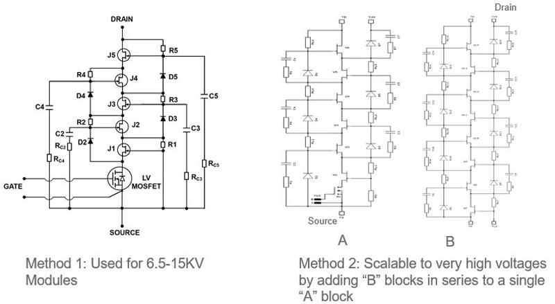
A second circuit (b) with the same capacitor in each stage is used in switches up to 40KV.
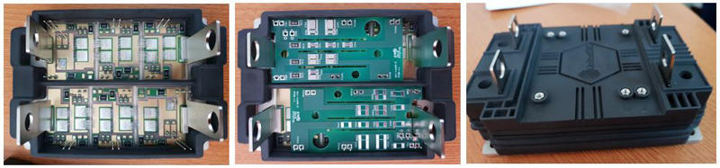
Most of the power is dissipated in SiC JFETs on the DBC substrate. The balance network is placed on the PCB board as it consumes less power.
Half-bridge modules feature very low conduction and switching losses. The Qrr is very low due to the recovery properties of Supercascode.
表3に示すように、電力損失はIGBTを使用した場合よりも劇的に低くなります。以降の段落では、これらの低損失がさまざまなアプリケーションに与える影響を調べます。
Supercascode can be used at ten times the frequency due to its low switching losses.
HV Switch Application: Medium Voltage Solid State Transformer
Solid state transformers typically convert medium and high voltage AC inputs (eg 4160V AC, 13.8KVAC) to lower voltage outputs without the use of bulky 60Hz transformers. The basic concept is shown in Figure 5, where AC voltage is first rectified and then converted to high power, high frequency AC in the 5-100kHz range. Smaller medium and high frequency transformers can reduce the secondary voltage and rectify it to supply the low voltage DC bus. This voltage can be used to drive a DC-AC inverter to charge a car or manage a low-voltage motor. Solid-state transformers are a fraction of the size of typical 60Hz transformers, and can distribute power at very high voltages and convert to lower voltages when used. This results in less current to distribute power, less copper weight and cost, and less loss. This is particularly effective at megawatt power levels, e.g. DC fast charging stations where 8-10 cars need to be charged at 250-350 kW, or large ships when distributing low AC voltages. Effective for reducing copper loss that occurs.
If the primary side rectified voltage exceeds 6KV and switching frequency above 500Hz-1KHz is required, 3.3KV-6.5KV class IGBT or IGCT cannot be used. Instead, the user has a multilevel inverter architecture with 7+ levels of 1700V IGBTs, or an MMC with many cascoded low voltage converters timed to provide a stepped sine wave output. You can choose to use a modular multi-level converter). Figure 6 shows an example of a modular multi-level converter, each stage of the converter uses a 3-level 1700V IGBT module on the primary side. Figure 7 shows a 3-level SiC configuration with a 10KV switch. Clearly, SiC configurations can simplify the architecture and control of such DC-AC converters and allow them to operate at relatively high frequencies.
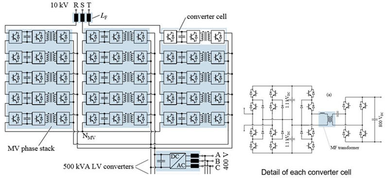
Inside each cascoded converter cell there is a 3 level 1700V module on the primary side. All these switches and all converters must be controlled to provide the desired output sine wave.
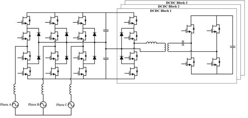
Control complexity and number of high voltage devices are greatly reduced. To use a small transformer, the switching frequency must be ten times higher than the silicon solution, and losses must be kept manageable so that thermal management is not complicated. This is where HV SiC devices excel.
megawatt class motor drive
According to a study of U.S. electricity use compiled by the DOE, 14% of all electricity generated is consumed by MW-class industrial motor drives. Using these motors in variable speed drives instead of direct grid connection can significantly reduce operating costs. These motor drives must operate at higher bus voltages to reduce operating currents and manage copper wire size and losses. Instead of using Si-based inverters operating from 500 Hz to 2 kHz, SiC-based inverters can be used at 10 times higher frequency, significantly reducing cooling needs and system size.
System designers can choose between the same multi-level converter architecture using silicon discussed in the last section, or a simpler 2-level or 3-level solution using SiC modules. . SiC can also be used to increase operating voltages, reducing upstream costs in power generation and distribution. However, to take full advantage of SiC's capabilities, significant developments in motor design and technology are required. However, even today, the benefits of SiC are well understood, such as improved motor operating efficiency due to reduced current ripple and improved inverter efficiency due to reduced loss. In some applications, using SiC allows the use of smaller, high-RPM motors, potentially eliminating the need for a Box.
Auxiliary power supply for high voltage systems
All of the above systems require low voltage for system control electronics (+/-5V, 12V, 24V) and small auxiliary lighting and cooling systems. Modules with lower current ratings with higher voltage capabilities help simplify this power from medium voltage AC. Applying the Supercascode concept to this application, the switch voltage can be easily scaled up. The normally-on characteristic of SiC JFETs in series with low-power normally-off MOSFETs can also be used to simplify start-up circuits, as demonstrated in low-power flyback converters. Depending on the power level, users can choose to use power modules or off-the-shelf JFET components for discrete configuration on the PCB.
HV DC breaker
With the prevalence of DC generation and DC loads, solid-state circuit breakers are replacing mechanical breakers for increased reliability, reduced size, reduced arcing concerns, and added intelligence for system protection. There is a renewed focus on how we use them. Solid-state breakers have no moving parts and do not attempt to mechanically cut current, making them immune to arcing concerns and mechanical wear of contacts. The main value for solid state in blocking DC current without forcing a resonant zero current crossing is that it can be easily done in less than 1ms. A much smaller disconnect switch can then be turned on with zero current, providing galvanic isolation. This method dramatically reduces the duration and magnitude of fault currents that downstream circuits and sources must contend with.
Figure 8 shows an example of the type of arrangement commonly used in solid-state circuit breakers with bidirectional functionality. In large power systems, cabling and load inductance can vary widely, so the energy stored in the line inductance must be dissipated when interrupting the DC fault current. This energy can be so large that it is dissipated by the MOVs used in parallel in Figure 8. A snubber circuit mitigates dV/dt and di/dt during turn-off.
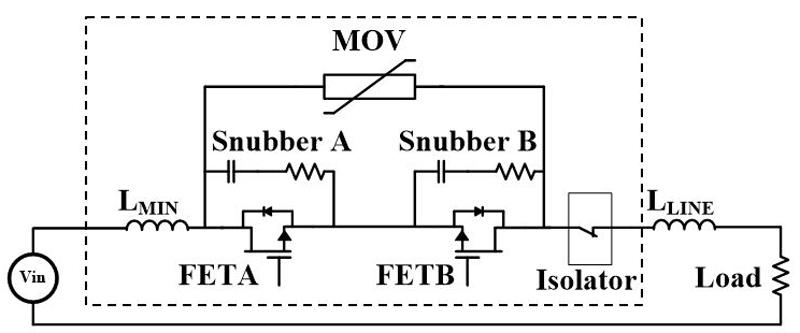
A back-to-back switch provides standoff voltage in either direction. RC snubbers soften switching voltage transitions. The MOV is sized to dissipate the stored worst-case energy of the line inductance. Supercascode switches can handle virtually any level of voltage or current.
The main requirements for switches used in this application are low conduction losses, ease of voltage and current scaling, and robust behavior during turn-off at high fault currents. Again the Supercascode approach works well here. SiC JFETs, with their good temperature coefficient of on-resistance and nearly flat VTH over temperature, are very easy to parallelize, making high current scaling very easy. The use of Supercascode technology also simplifies voltage scaling, allowing the breaker operation to be controlled by simply driving a low voltage MOSFET to one common source reference.
As shown in Figure 9, the use of a simple op amp circuit in combination with low-voltage MOSFET Supercascode provides a fast-acting current breaker with very low insertion loss while minimizing the peak fault current. I can. This type of circuit can be modified to manage inrush current and trip only when an actual fault occurs. In this example, voltage scaling is done by series connected devices and current scaling is done in parallel stages.
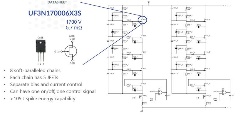
It consists of 8 parallel connected JFETs each with 5 series connected JFETs. The trip current can be set using the op amp voltage reference. Current can be sensed as shown or using the VDS(ON) of a low-voltage MOSFET.
Conclusion
SiC devices are excellent candidates for improving power electronics on medium and high voltage applications. From solid-state transformers to megawatt-class motor drives, auxiliary power systems to solid-state circuit breakers, SiC MOSFETs in general and SiC JFET-based Supercascode in particular offer highly attractive high performance and simplified systems. indicated to provide. The growth of these applications will drive the growth of SiC-based power electronics in the future, well beyond the EV boom of the 2020s.
Inquiry
If you have any questions regarding this article, please contact us below.
Qorvo manufacturer information top page
If you want to return to Qorvo manufacturer information Top, please click below.
