- Semiconductor BusinessHOME
- Products and Services of Macnica,Inc.
-
technical information

-
Events and Seminars
- Handling Manufacturer
- Support
- Inquiry
- Click here to purchase products
- Semiconductor business e-mail magazine registration
![]()
![]() Narrow down by specifying conditions
Narrow down by specifying conditions
現在2179件がヒットしています。check

Overview
High-frequency switches using wide bandgap semiconductors contribute to the efficiency of power conversion. Silicon carbide switches, for example, can be implemented as SiC MOSFETs or as SiC FETs in a cascode configuration.
This article traces the origins of SiC FETs, their evolution to the latest generation, and compares their performance with other technologies. In four installments, I will discuss the differences in physical characteristics, approaches and features for ideal switches, reliability, and unique uses in real-world applications.
SiC Cascode JFET – An Alternative Approach
With the advent of wide bandgap technology, many semiconductor manufacturers have chosen to develop SiC MOSFETs using their existing manufacturing lines, while others have chosen to start from a "clean slate" and explore other options. The simplest switch using SiC is the JFET structure, which has no gate oxide and is a unipolar conduction device, so it does not have the limitations of MOSFETs.
However, this device has a major drawback: it is "normally on" when the gate drive is 0V, and requires a negative drive to turn it off. This is inconvenient, especially under transient conditions such as turning the system on and off, and in the worst case leads to application failure. The SiC cascode JFET is a combination of a SiC JFET and a silicon MOSFET that is normally off but maintains the advantages of the JFET over a MOSFET. Figure 1 compares the layout of a SiC cascode JFET (right) with the schematic of a typical SiC MOSFET (left).
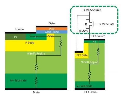
The SiC cascode JFET arrangement is called a cascode, and may be familiar to adult engineers who have seen the prototype vacuum tube combinations intended to reduce noise in audio amplifiers. Cascodes or "emitter switches" have appeared in various forms over the years, including bipolar transistors and BJT/MOSFET combinations, but their common feature is that a low-voltage switch controls a high-voltage switch, providing a good compromise between high voltage rating and ease of drive. However, circuits using BJTs have not been popular at high power due to their large base drive currents and slow switching speeds. The solution to these problems is the SiC cascode, or "SiC cascode JFET".
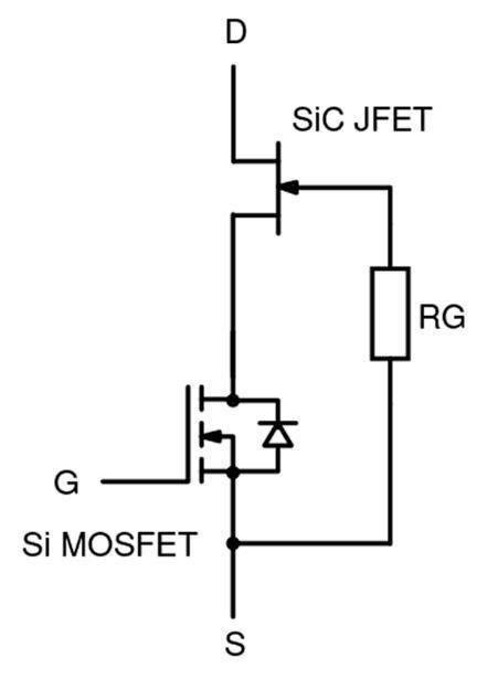
Referring to the circuit diagram of the SiC cascode JFET in Figure 2, when the Si-MOSFET is turned on through the gate, the source and gate of the JFET are effectively shorted and the JFET conducts. At this time, the on-resistance of the low-voltage Si-MOSFET can be made very small compared to the on-resistance of the high-voltage SiC FET, so current flows between the drain and source of the JFET and the MOSFET while keeping the conduction loss of the JFET fixed. When the Si-MOSFET is turned off, the source voltage of the JFET rises and exceeds the gate-source threshold (several volts negative), turning off the JFET. Due to the capacitance ratio of the device, the voltage of the Si-MOSFET remains low dynamically.
SiC cascode JFETs have many advantages over SiC MOSFETs, both in electrical performance and practicality. As a switch, the on-resistance is a major factor, but SiC cascode JFETs have a very high electron mobility in the channel compared to SiC MOSFETs. In addition, the channel density is high, so for the same area die, the on-resistance of the SiC cascode JFET is 2 to 4 times higher, and conversely, for the same on-resistance, you can get up to 4 times the number of dies compared to SiC MOSFETs. Compared to silicon superjunction MOSFETs, you can get up to 13 times the number of dies. Since silicon carbide as a material is likely to always be more expensive than silicon, increasing the number of dross dies per wafer is essential to the success of SiC cascode JFET technology. As we have said, the metric for measuring the viability of a die is the RDSA, which is a figure of merit.
Another benefit is the trade-off between RDS*EOSS, the on-resistance and the output switching energy of the device, given by the output capacitance. This is a useful metric because paralleling more cells in a die can reduce the on-resistance and conduction losses. However, this not only increases the area, but also directly increases the capacitance, which in turn increases EOSS, resulting in increased frequency-dependent switching losses. Therefore, a smaller RDS*EOSS value is advantageous.
The gate of a SiC cascode JFET is the same as the gate of the cascaded Si MOSFET. Therefore, it can be easily driven at 12V or 15V for full enhancement and low RDSON, with a large margin up to the absolute maximum of 25V. The gate drive of a SiC cascode JFET is also nominally compatible with silicon MOSFETs and IGBTs, ensuring backward compatibility when upgrading designs of existing products. In practice, SiC MOSFETs and GaN HEMT cells require a custom drive scheme for optimal efficiency and sufficient protection against overvoltage on the gate.
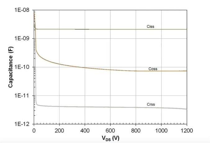
SiC cascode JFETs have very little gate-drain or "Miller" capacitance Crss due to the small device dimensions and the insulating effect of Si MOSFETs in a cascode arrangement, allowing for very fast switching. The output capacitance COSS and the associated switching energy EOSS are also small, allowing for fast switching with minimal losses. Due to the very fast edge rates, practical circuits require SiC cascode JFETs to be slowed down to reduce voltage overshoot and EMI. This can be done by adding a gate resistor, but this introduces unacceptable control delays at high switching frequencies, so a simple RC snubber is often a better solution. The capacitor is typically set at about 3×COSS, minimizing losses in the series resistor. Figure 3 shows the capacitance of a typical SiC cascode JFET device versus the change in drain voltage in the blocking state. The formulas for calculating the respective capacitance values are as follows:
・Ciss = CGS + CGD
(CDS is short)
・Crss = CGD
・Coss = CDS + CGD
SiC Cascode JFET "Body Diode"
Power converters require perfect switches to conduct in both directions with low losses. This is what is actually required in circuits such as AC motor drives and converters with inductive loads, so-called "third quadrant" operation. IGBTs cannot do this and require a parallel diode, but silicon or SiC based MOSFETs and JFETs can conduct in either direction through their channel under the control of the gate.
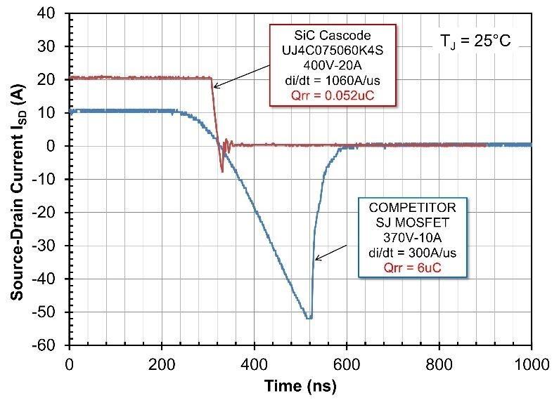
MOSFETs also have a built-in body diode that JFETs do not have, and in hard-switched converters with inductive loads, this body diode automatically conducts by "rectification" during the "dead time" before the device's channel is turned on through the gate, allowing current to flow in the reverse direction. This conduction allows a charge, Qrr, to be stored and then recovered when the body diode is reverse-biased.
This operation consumes large peak power, and the average value increases as the frequency increases, reducing efficiency. In silicon-based MOSFETs, this effect is so large that it may be practically unusable in circuits operating in Continuous Conduction Mode (CCM), such as a typical totem-pole PFC stage. SiC MOSFETs have Qrr values on the order of 10 times that of Si, but SiC cascode JFETs are even better because of the smaller output capacitance of the device and the smaller stored charge of the low-voltage MOSFET. Comparisons vary by device voltage class, but Figure 4 shows a typical reverse recovery plot of a silicon superjunction MOSFET similar to a SiC cascode JFET.
Although SiC MOSFETs and GaN devices have low or no reverse recovery losses, reverse conduction voltage drop is another story. This causes significant losses during dead time in power converters. Si superjunction MOSFETs typically exhibit a diode drop of around 1V, and SiC MOSFETs are even worse because they have a body diode that can easily drop 4V. A GaN HEMT cell operating in the third quadrant drops Vsd, which is the sum of the I*R channel voltage and the gate threshold voltage minus the gate-source voltage. The formula for Vsd is:
・Vsd = (Vth-Vgs) + (Isd*Ron)
GaN has a gate threshold of typically 1.5V, resulting in a large total drop at high currents. Typically, when the gate is driven negative to turn it off, this voltage Vgs is added to the source-drain drop, resulting in a Vsd of several volts, which can be significantly worse than other technologies. SiC cascode JFETs also experience an I*R drop due to channel resistance when conducting source-drain, just like GaN devices, but this drop is only increased by the voltage across the body diode of the low-voltage cascoded Si MOSFET, making it relatively low. As a result, the forward voltage drop is typically around 1.5V, which is better than the performance of SiC MOSFETs and GaN.
Inquiry
If you have any questions regarding this article, please contact us below.
On Semiconductor Manufacturer Information Top Page
If you want to go back to ONSEMI maker information top page, please click below.