- Semiconductor BusinessHOME
- Products and Services of Macnica,Inc.
-
technical information

-
Events and Seminars
- Handling Manufacturer
- Support
- Inquiry
- Click here to purchase products
- Semiconductor business e-mail magazine registration
![]()
![]() Narrow down by specifying conditions
Narrow down by specifying conditions
現在2182件がヒットしています。check

hello! I'm Ryosu, a new engineer on the Lattice team.
Last time, I created an SPI communication module in RTL design.
This time, we will simulate the created module and check the waveform and actually check it with the actual machine!
For those of you who are visiting this blog for the first time, let me give you a brief overview of this blog.
In this blog, I will introduce the process of making a temperature sensor that controls 7 segments with FPGA.
(If you're interested, I'll attach links to other episodes below, so please take a look!)
How important is simulation?
Suppressing the temptation to immediately evaluate the RTL design that I have worked so hard on on the actual device, I perform waveform simulation.
By performing a waveform simulation, you can check whether you have created the ideal waveform you intended.
Lattice Diamond comes with Mentor's Model Sim for Lattice Edition (LE) tool.
Waveform simulation will be performed using this Model Sim for LE.
Simulation and testbench
In order to perform a simulation, a module for simulation called a testbench is required in addition to the circuit you created.
This testbench is a description of the signals and conditions to be given to the circuit you have created.
I think it's gibberish if I just explain it in words, so I made an image diagram below!
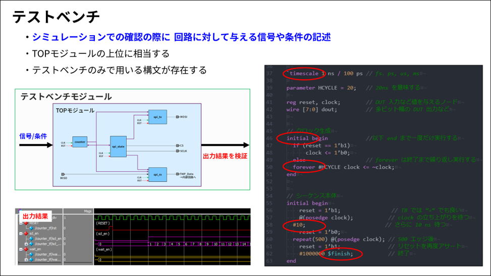
In this way, it is an image where the testbench module is one level higher than the TOP module you created.
The statements in the testbench have their own syntax, like the source code on the right.
Use this to input your intended signals and conditions and observe the output results (waveforms).
Generate testbench and launch Model Sim
Although it is rough, can you imagine the waveform simulation and the test bench?
From here, I will explain how to generate a testbench in Diamond and how to create a Model Sim foe LE project.
It's a template, but you can easily generate a testbench!
Testbench has a function to easily create a template on Diamond!
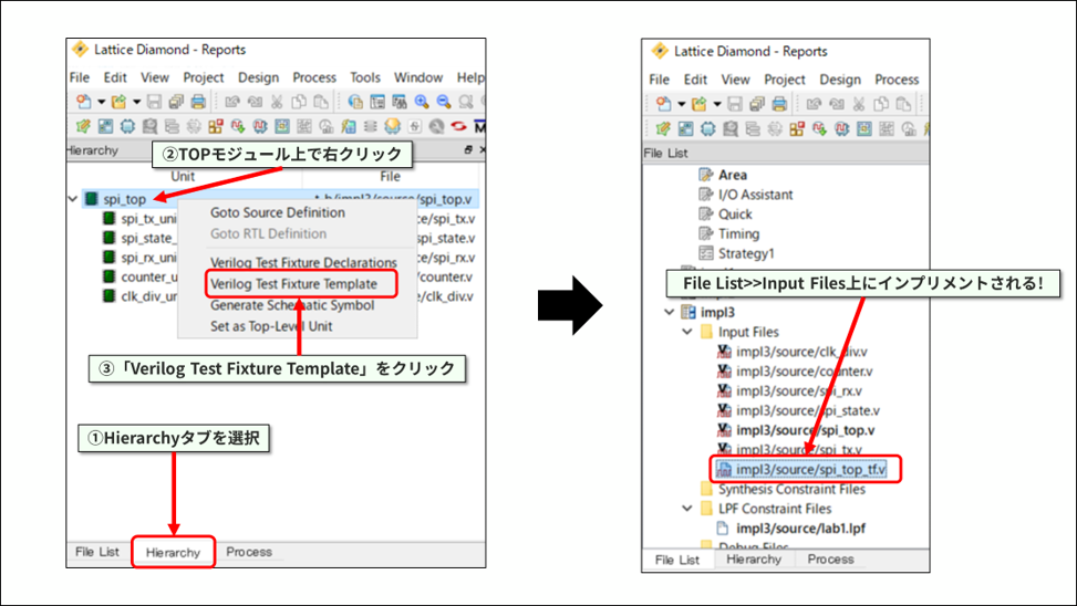
Go to Diamond >> Hierarch tab, right click on Top module,
By selecting the Verilog Test Fixture Template, it will appear on the File List >> Input Files.
Describe input signals and conditions in the generated template.
I will share the testbench file for easy waveform simulation!
Generate Model Sim Project from Diamond!
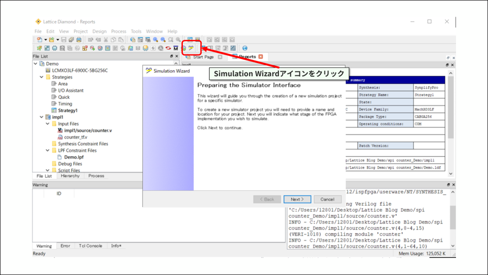
After creating the testbench, it's time to simulate.
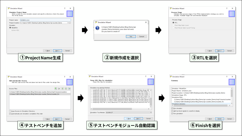
You can easily create a project in 5 steps from Diamond >> Simulation Wizard.
① Decide on a project name
② Select New
(3) Select RTL
④ Add testbench
⑤Automatic recognition of testbench
After creating the project, Model Sim for LE will launch automatically.
If you want to know how to operate Model Sim for LE in detail, please check the URL below!
Check the created RTL module with a simulation waveform
This is a little long explanation, but from here we will observe the waveform of the module created by Ryosu.
SPI_STATE module waveform observation
First, we will observe the waveform of the spi_state module.
After releasing RESET, the state machine transitions based on clk_div.
Progress through the states smoothly, return to the 16th state after the first 18th state, and repeat 16→17→18→16.
After Chip Select fell, SCLK started to move, and there seems to be no problem with the relationship between Chip Select and SCLK!
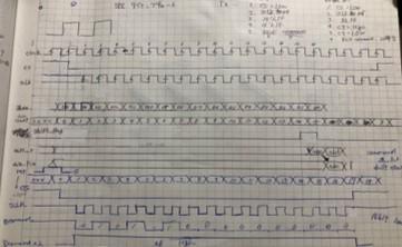
To be honest, this module was the most difficult... It took me about a week to get the ideal waveform. . .
I took the trouble to write waveforms on drawing paper, and rewrote the RTL based on that, and as a result, I was able to create an ideal waveform.
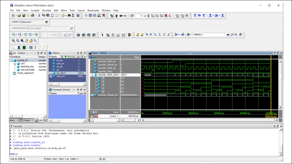
COUNTER module waveform observation
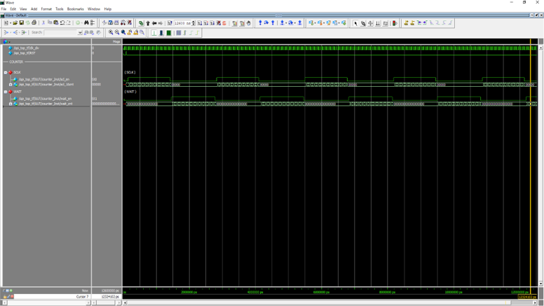
Next is the counter module. I was able to make this in one go!
The counter spins along with the Enable signal. This time, I reduced the number of counters for debugging and checked if there were any problems with the waveform.
SPI_TX module waveform observation
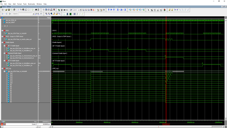
Next is the spi_tx module. I think this was the second most difficult part after spi_state.
Store the value in the register along with the Enable signal and output it serially using the shift register.
There seems to be no problem with the shift register, but I am a little worried. I'm looking forward to checking the actual machine. . .
SPI_RX module waveform observation
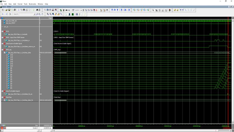
Next is the spi_rx module.
Move the shift register along with the Enable signal. Latch incoming data on the falling edge of SCLK.
After latching the data, store the value in another register and finalize the data.
This time, the testbench module is entering 16b'0000101100010000.
Looking at the register values after the data is fixed, it seems that the same values are stored!
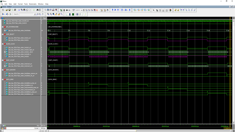
SPI_TOP module waveform observation
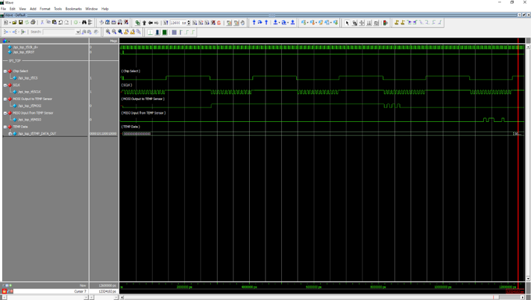
Finally the spi_top module.
It simulates a series of flows from after RESET is released to when data is received.
All 0 → All 1 → Command transmission → It seems to be a circuit that works like data reception! Was good! !
By the way, if the waveform simulation is not successful,
Strangely undefined, state does not transition, counter does not run, value is not saved in register, etc.
Various phenomena occur. By checking from each module instead of simulating from the TOP module at once
Makes it easier to find small mistakes. (Senior F-san taught me this!)
It seems that there is no problem even if you see the series of movements with the spi_top module, so next time I would like to check the operation on the actual machine.
Actual machine debugging, and,,,
Waveform simulation is over, and now it's time to check on the actual machine.
In the actual machine confirmation, using the internal node observation tool "Reveal Analyzer" attached to Diamond
Look at the register after the data is fixed and check if the data is close to the room temperature.
Observing internal nodes using Reveal Analyzer
Follow the steps below to observe internal nodes.
① Make various settings with Reveal Inserter and load it into the Diamond project
② Compile again up to Export Files
③After compiling, launch Reveal Analyzer
④Observation start
A design (Reveal core) for observing internal nodes is added to an existing design.
It uses about 300LUT resources. Be careful with resources.
If you want to know how Reveal works in detail, please check the materials below!
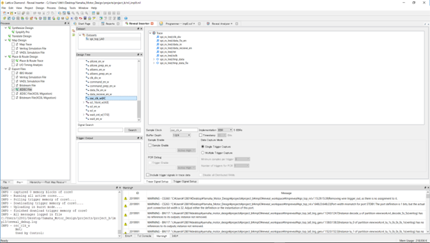
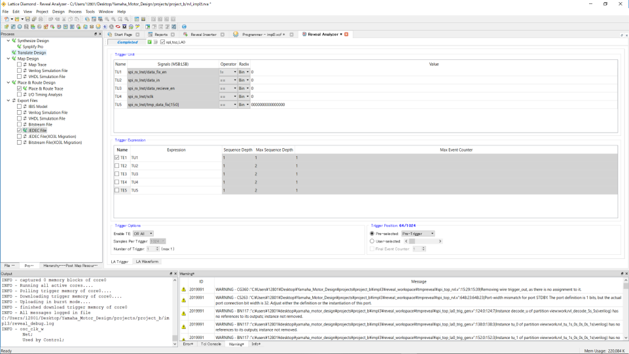
Select the signal you want to observe. After that, select the sampling clock and add observation conditions.
This time, I want to see the register after the temperature data is fixed, so I added a signal that seems to be related to this register as a condition.
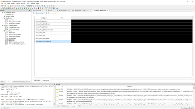
Check the design rules, and if there are no problems, add the Reveal file to the Diamond Project and compile.
Write the design file to the FPGA with the Dimaond Programmer and finally observe the internal nodes! (Throb)
To see the register after fixing the temperature data, observe the enable signal "tmp_data_fix_en" as a trigger condition.
The trigger condition is "Observe when transition from Low to High".
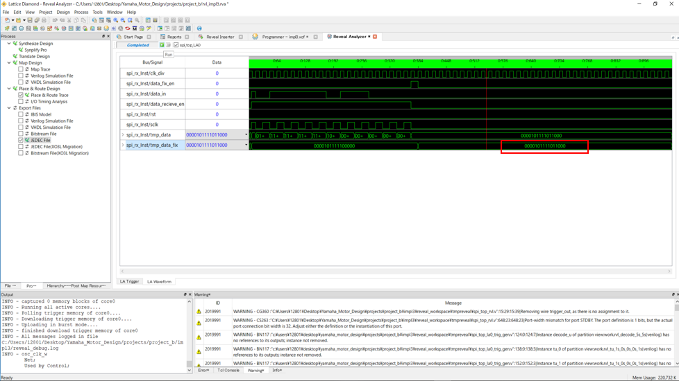
We were able to observe it safely under the trigger conditions! Do you really have temperature-like data?
The 16-bit binary data after data determination is "0000101111011000".
When I corrected the temperature, it turned out to be 23°C, which is close to room temperature! !
This took a long time - good! ! !
I observed it several times, but it seems that I can get the temperature information safely!
This time, we performed a waveform simulation of the created RTL module and confirmed it on the actual machine.
As an impression,
Debugging is hard! smile
For about a week, I repeated the process of checking the waveform → finding something wrong → correcting the RTL → checking the waveform.
However, there is a great sense of accomplishment when you do well. It seems to be addictive!
Next time, we will consider a circuit to display the acquired temperature data on a 7-segment LED display.
See you next time! See ya!