- 半導体事業HOME
- マクニカの製品・サービス
-
技術情報

-
イベント・セミナー
- 取扱メーカー
- サポート
- お問い合わせ
- 製品購入はこちら
- 半導体事業のメルマガ登録
![]()
![]() 条件を指定して絞り込む
条件を指定して絞り込む
現在2168件がヒットしています。check

こんにちは!Latticeチーム新人エンジニアのりょすです。
前回は、SPI通信についてどんな信号なのか、どのよう波形をしているのか調べました。
今回は、実際にSPI通信をVerilog-HDLにてRTL設計をおこなっていきたいと思います!
初めてこのブログを拝見していただいた方にこのブログの概要を少し紹介します。
このブログでは、温度センサー、7セグをFPGAで制御するものを製作する過程を紹介していきます。
(もし興味があったら、下に他の回のリンクを添付するので見ていただけると嬉しいです!)
SPI通信モジュールを考えてみる
前回、SPI通信について調べどのような波形で送ればいいのか理解することができました。
今回から実際にRTL設計をおこなっていくのですが、まず初めにモジュール全体の構成から検討していきたいと思います!
今回この仕様を実現するために使用する、使い勝手の良いFPGAの情報は以下よりご確認ください!
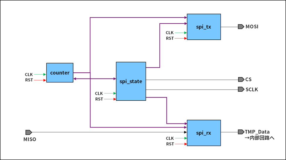
SPI通信モジュール全体構成
SPI通信のモジュール全体の構成を考えるにあたって、機能を分けていきます。
今回作成するSPIモジュールの機能は以下表のように大きく4つに分けます。また、ざっくりではありますが全体構成をイメージしてみました!
| モジュール名 | 説明 |
| spi_state | ステートの制御をおこなう |
| counter | 16bitとwait時間を数える |
| spi_tx | 温度センサーにコマンドを送信する |
| spi_rx | 温度センサーからの出力を受信する |
すぐやってみる!のも大切だとは思いますが、後のデバッグの際に「どういう意図で設計したっけ?」と忘れて大変にならないように
大枠から、TOPモジュールでの役割→各モジュールでの役割(機能)→各モジュールで必要な構文のように考えていきたいと思います。
TOPモジュールでの役割は、大まかに上記の表の4つとします。
spi_stateモジュールは、このSPI通信を実現させるための1番重要なモジュールとなります。
SPIのステートの状態を制御するモジュールです。
counterモジュールは、名前の通り必要な時にカウントするモジュールとなります。
spi_tx/rxモジュールは、spi_stateのステート状態を見て送受信を決定します。
なお、各モジュールのRESETは共通、入力クロックは内部オシレーターからの2.08MHzの出力を
Clock Deviederを用いて1/4分周した500kHzクロックを用います。(内部オシレーターとDeviderも後の章で説明します。)
各モジュールの詳細を考えてみる
ここから各モジュールの詳細な設計をおこなっていきたいと思います。
波形を再現するために、どのような役割や構文が必要かを考えていきます!
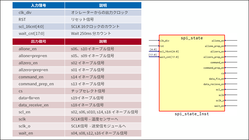
spi_stateモジュールの詳細
まず、spi_sateモジュールです。
このspi_stateモジュールは、SPI通信のステート状態を制御するモジュールとなります。SPI通信の動作を分解していき、1つのステートで1つの動作となるようにします。
分解した各ステートに沿って、他のモジュールが動作をおこなうため、このモジュールは、SPI通信の中核を担うようなモジュールとなります。
ヒトで言う、脳みそのようなものですね!
例えば、ステート1は CS = Low にするステート
ステート2は 温度センサーへコマンドを送信するステートのように1つの動作ごと分解します。
注意としては、細かくしすぎるとソースコードが長くなってしまいミスや、デバッグの際に大変になることがあります。
なので、今回は1つの動作につき1ステートの細かさで分けることにしました。
spi_state.vの詳細機能と、ステートを以下にまとめました。
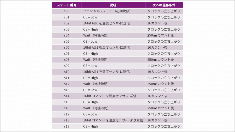
同じステートがいくつかあったり、遷移条件がバラバラなのはいいのか?少し考える必要がありそうですが
今回はこのステートと、遷移条件で設計を進めていきたいと思います。
このステートマシンモジュールでは、以下のの3つの機能を実現します。
①ステートの管理
②それぞれのステートの状態を教えるフラグの出力
③SCLKの出力
今回の記事では、各モジュールのソースコードを公開しています!
もし、気になる方がいましたらクリックすると別ウィンドウに表示されます。
(ド素人が全力で考えたソースコードでよければぜひ見ていただけると幸いです、、、)
このspi_stateモジュールの機能を実現するためのポイントを解説します。
①ステートの管理
→ステートの管理は、CASE文を用いて行います。デバッグを行い易くするために各ステートをパラメーター化をおこない、ある条件にてステート(CASE)が進んでいきます。
何かエラーがあったり、最終ステートまで進んだ際は、一番最初のステートに移行するようになっています。
私が作成したステートは、重複しているステートが多くもう少し簡略化できるのでは?と考えています。。。
②それぞれのステートの状態を教えるフラグの出力
→フラグは、イネーブル信号としてセレクター構文を用いています。ある条件になったらHigh出力、それ以外はLow出力とします。
③SCLKの出力
→SCLKは、カウンター回路を用いてHigh/Low出力をおこないます。あるステートにいる場合に、カウンターを動かしてSCLKを出力します。
counterモジュールの詳細
次にカウンターモジュールです。
このモジュールでは、SCLK 16クロック分のカウントと、Waitの250ms分のカウントをおこないます。
counter.vの詳細機能は以下になります。
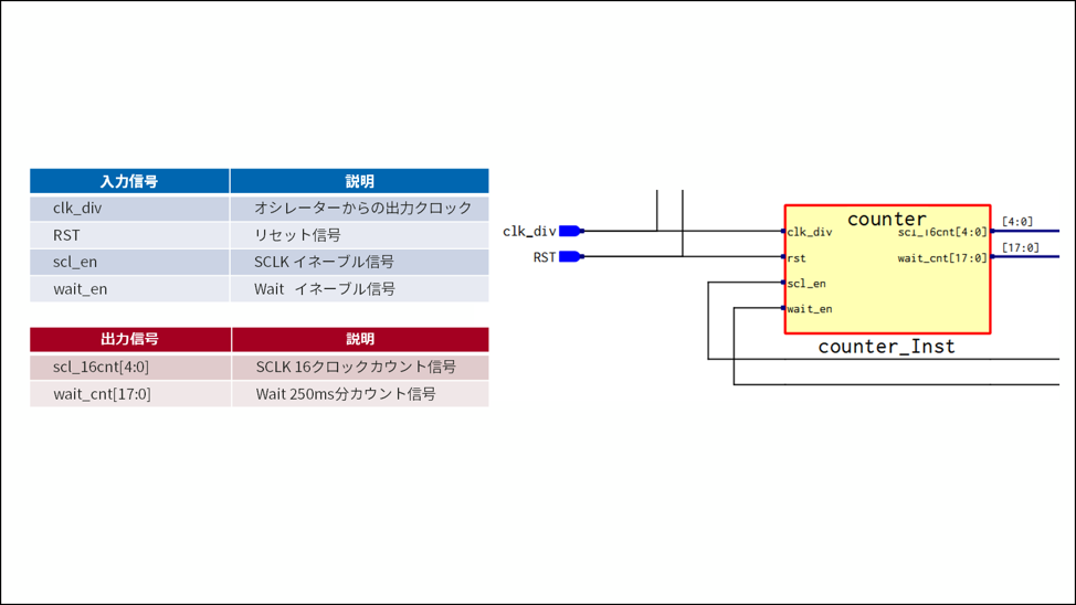
このモジュールは、spi_state からのイネーブル信号の状態(イネーブル信号がHighの時)によってカウンターをまわす機能を実現します。
カウントをspi_stateへ送り、ある一定の数までカウントをおこなうとspi_stateのステートが遷移し、同時にイネーブル信号が Lowとなります。
イネーブル信号が Lowになると、カウンターがリセットされます。
spi_txモジュールの詳細
このspi_tx.vは、温度センサーへコマンドを送信するモジュールとなります。
spi_tx.vの詳細機能は以下となります。
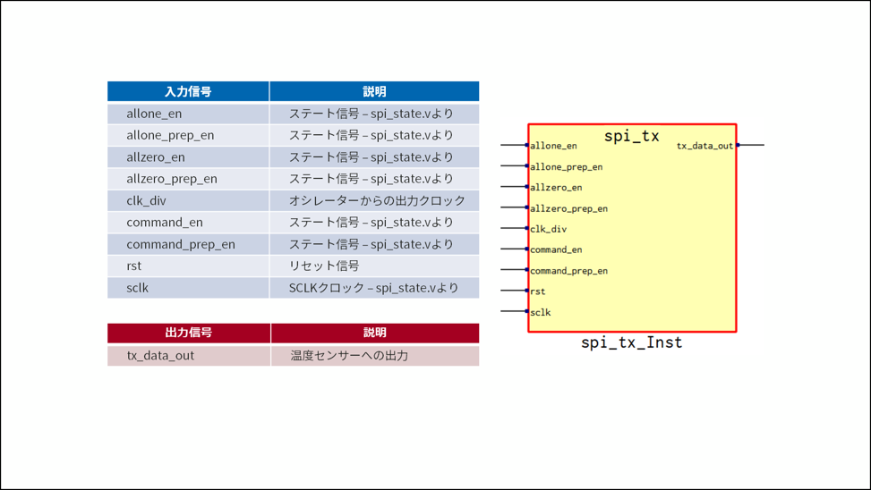
このモジュールでは、以下のの3つの機能を実現します。なお、spi_stateモジュールらのイネーブル信号によって動作します。
①送信する1つ前のステートでコマンドをレジスタにセットする
②送信するステートで、シフトレジスタ回路を動作させる
③パラシリ変換を行い、温度センサーへコマンドを送る
シフトレジスタってどうやって記述すればいいの? と一見難しそうに思いますが、意外と簡単に記述することができます!
このモジュールの機能を実現するためのポイントを解説します。
①送信する1つ前のステートでコマンドをレジスタにセットする
→レジスタを用いて、自分の意図したコマンドやALL 0/1をセットします。
②送信するステートで、シフトレジスタ回路を動作させる
③パラシリ変換を行い、温度センサーへコマンドを送る
→ソースコード、確認いただけましたでしょうか?
前のステートでセットしたデータを "addr[15:1] <= addr[14:0];" のように1行の記述でシフトレジスタでパラシリ変換ができてしまうのです!
ステートマシンのモジュールの記述がだいぶ汚かったので、今回スッキリ記述できて感動しています。。
spi_rxモジュールの詳細
このspi_rx.vは、温度センサーからの出力データを受信するモジュールとなります。
spi_rx.vの詳細機能は以下となります!
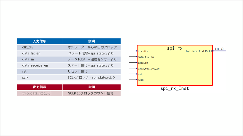
このモジュールでは、以下のの3つの機能を実現します。なお、spi_stateモジュールらのイネーブル信号によって動作します。
①データを受信するステートで、シフトレジスタを動作させる
②データを全て受け取ったら、データを確定させる
③次のモジュールへデータを送る
先ほどのspi_txモジュールと異なり、次はシリパラ変換をおこないます。こちらも簡単に記述することができます!
このモジュールの機能を実現するためのポイントを解説します。
①データを受信するステートで、シフトレジスタを動作させる
→パラシリ変換の記述と記述の仕方が若干異なりますが、こちらも1行で書くことができました!
②データを全て受け取ったら、データを確定させる
③次のモジュールへデータを送る
→データを受け取るステートの後に、保存用のレジスタに格納して次のモジュールへデータを渡します。
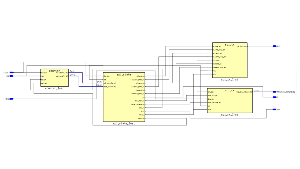
spi_topモジュールの詳細
最後にトップモジュールとなります!
トップモジュールでは、spi_state.v、counter.v、spi_rx.v、spi_tx.vの4つのモジュールを繋げます。
イメージは、大きな箱の中にそれぞれの小さい箱を詰めていくようなイメージです。
これを階層設計といいます。
階層設計をおこなうことで、コードが見やすくなったり、デバッグがおこないやすくなるなどの効果があります。
各4つのモジュールを呼び出して、トップモジュールに記述をおこないます。
このことをインスタンス化といいます。
また、トップモジュールに内部オシレーターとClock Deviderを呼び出す記述をおこないます。
トップモジュールでは、3つの機能を実現します。
①各モジュールのインスタンス化
②Clock Deviderの呼び出し
③内部オシレーターの呼び出し
トップモジュールの機能を実現するためのポイントを解説します。
①各モジュールのインスタンス化
→こちらは、wireによって各モジュール間を繋いでいきます。単純な記述ですが、意外と記述ミスするので注意して記述します。
②Clock Deviderの呼び出し
→Lattice FPGAではRTL記述によって呼び出すことができます。今回は1/4倍に分周するで各種設定RTLで記述します。
③内部オシレーターの呼び出し
→同様に、2.08MHzを出力するようにモジュールを呼び出します。
ただ、内部オシレーターは精度が±5%となっているのでより精度を求める場合は外部からクロックを入力するのがおすすめです。
今回は、SPI通信をRTLにて設計しました。
感想としては、
一見、複雑そうな通信も分解していくと構文の組み合わせが見えてくるので楽しかったです!
楽しかったとはいえ、Verilogとはなんぞや?というところから設計を始めたので、丸4日かかりました!笑
次回はModel Sim Lattice Eddtionを用いてシミュレーションをおこない、問題なさそうであれば実機での確認をおこないたいと思います!
では、また次回!See ya!

Lattice FPGA 入門ブログについて
全記事を通して、温度センサーにて取得した温度(SPI通信)を、FPGA内部で変換して7セグLED表示器に表示するモジュールを製作しています!
もし、「この新人君は何を作っているんだろう?」と興味を持っていただいた方がいましたら
ぜひ以下ページより、モジュールの制作過程や全体像をチェックいただけると嬉しいです!