- Semiconductor BusinessHOME
- Products and Services of Macnica,Inc.
-
technical information

-
Events and Seminars
- Handling Manufacturer
- Support
- Inquiry
- Click here to purchase products
- Semiconductor business e-mail magazine registration
![]()
![]() Narrow down by specifying conditions
Narrow down by specifying conditions
現在2184件がヒットしています。check

Metastability due to the connection of signals between different clock domains (CDC (Clock Domain Crossing)) is a problem in today's FPGA designs. Conventional structural verification alone is not effective for verifying CDC signals. This column will be divided into four parts to explain the CDC problem and how to verify it.
- Part 1: What is setup time and hold time?
- Part 2: What is Metastable?
- Part 3: General measures against metastability and their problems
- Part 4: How to verify metastable
Part 1: What is setup time and hold time?
All FFs (flip-flops)/registers built into LSIs such as FPGAs and ASICs have timing constraints such as setup and hold times so that they can correctly take in data at the time of input and generate output signals. is defined.
That is, the input data must be stable for a minimum time before the clock edge (setup time tCO) and a minimum time after the clock edge (hold time tH).
This time, I would like to explain the reason why there are restrictions on setup and hold time from the structure of D-FF (flip-flop). If the data is not stable at this point, not only do we not know which data will be taken before or after, but metastability occurs where the output stays at an intermediate potential between ``Low (0)'' and ``High (1)'' for a while. . So there is a setup/hold time constraint.
Let's take a closer look at this phenomenon.
There are various types of D-FF (flip-flop) structures, but CMOS circuits generally consist of inverters, transfer gates, etc., as shown in Figure 1-1. It is different from the D-FF circuit diagram written in the textbook, but the logic is the same and the feature is that the number of transistors is small.
The transfer gate acts as a switch, turning it on or off depending on the state value of clock “C”.
There are loop circuits (latch circuits) using two inverters in the front and rear stages, and these are the mechanisms for holding data.
As for the operation, when the clock “C” is L (Low/0), the data “D” signal is read, and when “C” rises (↑), the data is output to the output “Q”.
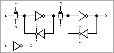
Figure 1-1 General D-FF circuit structure
Figure 1-2 is when "C" is L (Low/0).
The “D” signal is stored in the former inverter loop, and the previous cycle data is held in the latter inverter loop.
Since the transfer gate that connects the inverter loops in the previous stage and the latter stage is off, no signal is transmitted.
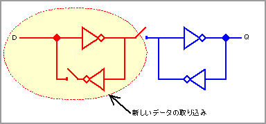
Figure 1-2 “C” is “Low (0)”
Figure 1-3 is when “C” is H (High/1).
When “C” is set to ↑, the data stored in the inverter loop of the previous stage is transmitted to the subsequent stage.
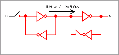
Figure 1-3 “C” is “Low (0)”
If "C" is set to ↑, no signal comes in from "D" as shown in Fig. 1-3.
At this time, if the signal does not make one round of the inverter loop in the previous stage, the signal fluctuates between "L" and "H" and becomes an intermediate potential (metastable). Of course, since it is a CMOS circuit, it goes “L” or “H” after a certain amount of time, but since the metastable state is longer than the delay time, data may be lost.
Because of this, there are set-up time constraints.
Also, if "C" is turned up and "D" changes just before the input of "D" is closed, the data that should be taken in the next cycle can be taken in quickly, and in the same way, oscillation and metastability will occur in the inverter loop. will occur, so the signal of “D” must be stable for a while even after “C” becomes ↑.
Because of this, there is a hold time constraint.
Therefore, if there is only one clock, there is no problem as long as the setup and hold time constraints are observed. But you have to be careful when you have multiple clocks.
That's all for now. Next time, I will explain metastable.